
Datasheet


ADC0820-N
www.ti.com
SNAS529C –JUNE 1999–REVISED MARCH 2013
WR then RD Mode
With the MODE pin tied high, the A/D will be set up for the WR-RD mode. Here, a conversion is started with the
WR input; however, there are two options for reading the output data which relate to interface timing. If an
interrupt driven scheme is desired, the user can wait for INT to go low before reading the conversion result
(Figure 22). INT will typically go low 800 ns after WR's rising edge. However, if a shorter conversion time is
desired, the processor need not wait for INT and can exercise a read after only 600 ns (Figure 21). If this is
done, INT will immediately go low and data will appear at the outputs.
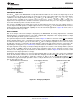
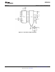
Figure 21. WR-RD Mode (Pin 7 is High and t
RD
<t
I
) Figure 22. WR-RD Mode (Pin 7 is High and t
RD
>t
I
)
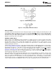
Stand-Alone
For stand-alone operation in WR-RD mode, CS and RD can be tied low and a conversion can be started with
WR. Data will be valid approximately 800 ns following WR's rising edge.
Figure 23. WR-RD Mode (Pin 7 is High) Stand-Alone Operation
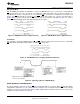
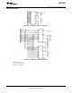
Note: MS means most significant
LS means least significant
Figure 24. Operating Sequence (WR-RD Mode)
OTHER INTERFACE CONSIDERATIONS
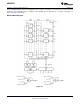
In order to maintain conversion accuracy, WR has a maximum width spec of 50 µs. When the MS flash ADC's
sampled-data comparators (see The Sampled-Data Comparator) are in comparison mode (WR is low), the input
capacitors (C, Figure 19) must hold their charge. Switch leakage and inverter bias current can cause errors if the
comparator is left in this phase for too long.
Copyright © 1999–2013, Texas Instruments Incorporated Submit Documentation Feedback 13
Product Folder Links: ADC0820-N