
Datasheet


ADC0820-N
www.ti.com
SNAS529C –JUNE 1999–REVISED MARCH 2013
FUNCTIONAL DESCRIPTION
GENERAL OPERATION
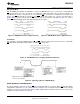
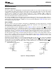
The ADC0820-N uses two 4-bit flash A/D converters to make an 8-bit measurement (Figure 3). Each flash ADC
is made up of 15 comparators which compare the unknown input to a reference ladder to get a 4-bit result. To
take a full 8-bit reading, one flash conversion is done to provide the 4 most significant data bits (via the MS flash
ADC). Driven by the 4 MSBs, an internal DAC recreates an analog approximation of the input voltage. This
analog signal is then subtracted from the input, and the difference voltage is converted by a second 4-bit flash
ADC (the LS ADC), providing the 4 least significant bits of the output data word.
The internal DAC is actually a subsection of the MS flash converter. This is accomplished by using the same
resistor ladder for the A/D as well as for generating the DAC signal. The DAC output is actually the tap on the
resistor ladder which most closely approximates the analog input. In addition, the “sampled-data” comparators
used in the ADC0820-N provide the ability to compare the magnitudes of several analog signals simultaneously,
without using input summing amplifiers. This is especially useful in the LS flash ADC, where the signal to be
converted is an analog difference.
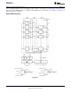
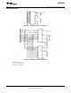
THE SAMPLED-DATA COMPARATOR
Each comparator in the ADC0820-N consists of a CMOS inverter with a capacitively coupled input (Figure 17
Figure 18). Analog switches connect the two comparator inputs to the input capacitor (C) and also connect the
inverter's input and output. This device in effect now has one differential input pair. A comparison requires two
cycles, one for zeroing the comparator, and another for making the comparison.
In the first cycle, one input switch and the inverter's feedback switch (Figure 17) are closed. In this interval, C is
charged to the connected input (V1) less the inverter's bias voltage (V
B
, approximately 1.2V). In the second cycle
(Figure 18), these two switches are opened and the other (V2) input's switch is closed. The input capacitor now
subtracts its stored voltage from the second input and the difference is amplified by the inverter's open loop gain.
The inverter's input (V
B
′) becomes
(1)
and the output will go high or low depending on the sign of V
B
′−V
B
.
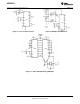
The actual circuitry used in the ADC0820-N is a simple but important expansion of the basic comparator
described above. By adding a second capacitor and another set of switches to the input (Figure 19), the scheme
can be expanded to make dual differential comparisons. In this circuit, the feedback switch and one input switch
on each capacitor (Z switches) are closed in the zeroing cycle. A comparison is then made by connecting the
second input on each capacitor and opening all of the other switches (S switches). The change in voltage at the
inverter's input, as a result of the change in charge on each input capacitor, will now depend on both input signal
differences.
• V
O
= V
B
• V on C = V1−V
B
• C
S
= stray input node capacitor
• V
B
= inverter input bias voltage
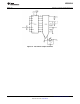
Zeroing Phase
Figure 17. Sampled-Data Comparator
Compare Phase
Copyright © 1999–2013, Texas Instruments Incorporated Submit Documentation Feedback 11
Product Folder Links: ADC0820-N