
Datasheet

ADC0820-N
SNAS529C –JUNE 1999–REVISED MARCH 2013
www.ti.com
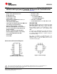
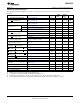
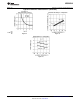
PIN DESCRIPTIONS
Pin Name Function
1 V
IN
Analog input; range =GND≤V
IN
≤V
CC
2 DB0 TRI-STATE data output—bit 0 (LSB)
3 DB1 TRI-STATE data output—bit 1
4 DB2 TRI-STATE data output—bit 2
5 DB3 TRI-STATE data output—bit 3
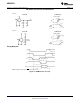
WR: With CS low, the conversion is started on the falling edge of WR. Approximately 800 ns
(the preset internal time out, t
I
) after the WR rising edge, the result of the conversion will be
WR-RD Mode
strobed into the output latch, provided that RD does not occur prior to this time out (See
Figure 5 & Figure 6).
6 WR / RDY
RDY: This is an open drain output (no internal pull-up device). RDY will go low after the falling
RD Mode edge of CS; RDY will go TRI-STATE when the result of the conversion is strobed into the
output latch. It is used to simplify the interface to a microprocessor system (See Figure 4).
Mode: Mode selection input—it is internally tied to GND through a 50 µA current source.
7 Mode RD Mode: When mode is low
WR-RD Mode: When mode is high
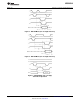
With CS low, the TRI-STATE data outputs (DB0-DB7) will be activated when RD goes low
(See Figure 7). RD can also be used to increase the speed of the converter by reading data
WR-RD Mode
prior to the preset internal time out (t
I
, ∼800 ns). If this is done, the data result transferred to
output latch is latched after the falling edge of the RD (See Figure 5 & Figure 6).
8 RD
With CS low, the conversion will start with RD going low, also RD will enable the TRI-STATE
RD Mode data outputs at the completion of the conversion. RDY going TRI-STATE and INT going low
indicates the completion of the conversion (See Figure 4).
INT going low indicates that the conversion is completed and the data result is in the output
latch. INT will go low, ∼800 ns (the preset internal time out, t
I
) after the rising edge of WR (See
WR-RD Mode
Figure 6); or INT will go low after the falling edge of RD , if RD goes low prior to the 800 ns
9 INT
time out (See Figure 5). INT is reset by the rising edge of RD or CS (See Figure 5 & Figure 6).
INT going low indicates that the conversion is completed and the data result is in the output
RD Mode
latch. INT is reset by the rising edge of RD or CS (See Figure 4).
10 GND Ground
11 V
REF
(−) The bottom of resistor ladder, voltage range: GND≤V
REF
(−)≤V
REF
(+)
(1)
12 V
REF
(+) The top of resistor ladder, voltage range: V
REF
(−)≤V
REF
(+)≤V
CC
(1)
13 CS CS must be low in order for the RD or WR to be recognized by the converter.
14 DB4 TRI-STATE data output—bit 4
15 DB5 TRI-STATE data output—bit 5
16 DB6 TRI-STATE data output—bit 6
17 DB7 TRI-STATE data output—bit 7 (MSB)
Overflow output—If the analog input is higher than the V
REF
(+), OFL will be low at the end of conversion. It can
18 OFL be used to cascade 2 or more devices to have more resolution (9, 10-bit). This output is always active and does
not go into TRI-STATE as DB0–DB7 do.
19 NC No connection
20 V
CC
Power supply voltage
(1) When the input voltage (V
IN
) at any pin exceeds the power supply rails (V
IN
< V
−
or V
IN
> V
+
) the absolute value of current at that pin
should be limited to 1 mA or less. The 4 mA package input current limits the number of pins that can exceed the power supply
boundaries with a 1 mA current limit to four.
10 Submit Documentation Feedback Copyright © 1999–2013, Texas Instruments Incorporated
Product Folder Links: ADC0820-N