
Datasheet

ADC0816, ADC0817
www.ti.com
SNAS527C –JUNE 1999–REVISED MARCH 2013
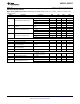
Absolute Maximum Ratings
(1) (2)
Supply Voltage (V
CC
)
(3)
6.5V
Voltage at Any Pin −0.3V to (V
CC
+0.3V)
Except Control Inputs
Voltage at Control Inputs −0.3V to 15V
(START, OE, CLOCK, ALE, EXPANSION CONTROL,
ADD A, ADD B, ADD C, ADD D)
Storage Temperature Range −65°C to +150°C
Package Dissipation at T
A
= 25°C 875 mW
Lead Temp. (Soldering, 10 seconds)
Dual-In-Line Package (Plastic) 260°C
Molded Chip Carrier Package
Vapor Phase (60seconds) 215°C
Infrared (15 seconds) 220°C
ESD Susceptibility
(4)
400V
(1) Absolute Maximum Ratings indicate limits beyond which damage to the device may occur. DC and AC electrical specifications do not
apply when operating the device beyond its specified operating conditions.
(2) All voltages are measured with respect to GND, unless otherwise specified.
(3) A Zener diode exists, internally, from V
CC
to GND and has a typical breakdown voltage of 7 V
DC
.
(4) Human body model, 100 pF discharged through a 1.5 kΩ resistor.
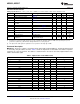
Operating Conditions
(1)
Temperature Range
(2)
T
MIN
≤T
A
≤T
MAX
ADC0816CCN, ADC0817CCN −40°C≤T
A
≤+85°C
Range of V
CC
(2)
4.5 V
DC
to 6.0V
DC
Voltage at Any Pin 0V to V
CC
Except Control Inputs
Voltage at Control Inputs 0V to 15V
(START,OE, CLOCK, ALE, EXPANSION CONTROL,
ADD A, ADD B, ADD C, ADDD)
(1) All voltages are measured with respect to GND, unless otherwise specified.
(2) Absolute Maximum Ratings indicate limits beyond which damage to the device may occur. DC and AC electrical specifications do not
apply when operating the device beyond its specified operating conditions.
Copyright © 1999–2013, Texas Instruments Incorporated Submit Documentation Feedback 3
Product Folder Links: ADC0816 ADC0817