
Datasheet


www.ti.com
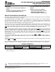
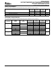
OPERATING CHARACTERISTICS
(1)
SN74ALVCH32973
16-BIT BUS TRANSCEIVER AND TRANSPARENT D-TYPE LATCH
WITH EIGHT INDEPENDENT BUFFERS
SCES436C – APRIL 2003 – REVISED SEPTEMBER 2004
T
A
= 25 ° C
V
CC
= 1.8 V V
CC
= 2.5 V V
CC
= 3.3 V
TEST
PARAMETER UNIT
CONDITIONS
TYP TYP TYP
One f
A
= 10 MHz,
One f
B
= 10 MHz,
A outputs enabled,
TOE = GND,
Q outputs disabled, 12 14 19
LOE = V
CC
,
one A output switching
DIR = GND,
C
L
= 0 pF
One f
A
= 10 MHz,
One f
B
= 10 MHz,
B outputs enabled,
TOE = GND,
Q outputs disabled, 12 14 21
LOE = V
CC
,
one B output switching
DIR = GND,
C
pd
(2)
Power dissipation
C
L
= 0 pF
pF
(each output) capacitance
One f
A
= 10 MHz,
One f
LE
= 20 MHz,
Q outputs enabled,
One f
Q
= 10 MHz,
A and B I/Os isolated, 11 13 19
TOE = V
CC
,
one Q output switching
LOE = GND,
C
L
= 0 pF
One f
D
= 10 MHz,
One Y output switching, One f
Y
= 10 MHz,
A and B I/Os isolated, TOE = V
CC
, 7 8 12
Q outputs disabled LOE = V
CC
,
C
L
= 0 pF
One f
A
= 10 MHz,
A and B I/Os isolated, One f
LE
= 20 MHz,
C
pd
Power dissipation Q outputs disabled, f
Q
not switching,
4 5 11 pF
(Z) capacitance one LE and one A data TOE = V
CC
,
input switching LOE = V
CC
,
C
L
= 0 pF
f
A
not switching,
One f
LE
= 20 MHz,
A and B I/Os isolated,
C
pd
(3)
Power dissipation f
Q
not switching,
Q outputs disabled, 6 7 9 pF
(each LE) capacitance TOE = V
CC
,
one LE input switching
LOE = V
CC
,
C
L
= 0 pF
(1) Total device C
pd
for multiple (m) outputs switching and (n) LE inputs switching = [m * C
pd
(each output)] + [n * C
pd
(each LE)]
(2) C
pd
(each output) is the C
pd
for each data bit (input and output circuitry) when it operates at 10 MHz (Note: The LE is operating at
20 MHz in this test, but its I
CC
component has been subtracted).
(3) C
pd
(each LE) is the C
pd
for the clock circuitry only when it operates at 20 MHz.
8