
User's Manual

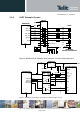


Table Of Contents
- 1 Introduction
- 2 General Product Description
- 3 Application Interface
- 3.1 Power Supply
- 3.2 Reset
- 3.3 Serial Interface
- 3.4 GPIO Interface
- 3.5 I2C Interface 0F
- 3.6 SPI Serial Peripheral Interface
- 3.7 Bluetooth Radio Interface
- 1.1
- 3.8 NFC Function
- 3.9 Slow Clock Interface
- 3.10 Test Mode
- 3.11 Operating in a Power-Switched Environment
- 3.12 Serial Wire Debug Interface
- 3.13 DC/DC Converter
- 4 Module Pins
- 5 Electrical Characteristics
- 6 Mechanical Characteristics
- 7 Application Diagram
- 8 Compliances
- 9 Packing
- 10 Ordering Information
- 11 Safety Recommendations
- 12 Document History

BlueMod+S42 Hardware User Guide
1VV0301303 Rev.3 – 2016-08-22
Reproduction forbidden without written authorization from Telit Communications S.p.A. - All Rights Reserved.
Page 30 of 62
To enter and use BlueMod+S42 Testmode or DTM, access to the following signals is
required:
• BOOT0
• TESTMODE#
• UART-RXD
• UART-TXD
• UART-RTS#
• UART-CTS#
• GND
These pins shall be routed to some test pads on an outer layer, but can be left open during
normal operation when not used.
Please note the UART is required for operation of test modes. During the homologation
process, UART-RXD, UART-TXD, UART-RTS# and UART-CTS# must be freely
accessible.
3.11 Operating in a Power-Switched Environment
A potential “back feeding” problem may arise, if the module is operated in an environment
where its power supply (VSUP) is switched off by the application. This might be done to save
some power in times Bluetooth is not needed.
As stated in Table 9, the voltage on any I/O pin must not exceed VSUP
by more than 0,3V at any time. Otherwise some current I
INJ
flows through the internal
protection diodes. This may damage the module (please refer to chapter 5.1 for limits).
There is no problem if the application circuit design and programming can assure that all
signals directed towards BlueMod+S42are set to low (U < 0,3V) before and while VSUP is
turned off. If this is not guaranteed, at least a series resistor (about 1k) must be inserted into
each signal path. This does protect the module but obviously cannot prevent from an
unwanted, additional current flow in case of such signal being at high-level. It may be
necessary to use driver chips in such applications, that gate off these signals while VSUP is
not present.
3.12 Serial Wire Debug Interface
The Serial Wire Debug (SWD) interface (signals SWDIO, SWCLK) is normally not used in a
customer’s product. It is reserved for debugging purposes.
Leave SWDIO, SWCLK unconnected. Only if you intend to use them for debugging
purposes, make them available.