
User's Manual
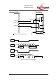
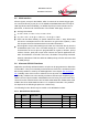
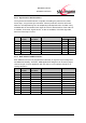
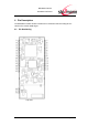
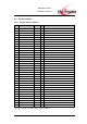
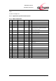
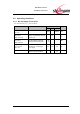
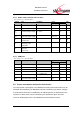
Table Of Contents
- Introduction
- Block Diagram
- Application Interface
- Pin Description
- Electrical Characteristics
- Mechanical Characteristics
- Approvals/Certifications
- Related Documents
- Ordering Information
- History

BlueMod+C11/G2
Hardware Reference
www.stollmann.de Page 13 of 42
3.6.2 Synchronous Serial Interface
The Synchronous Serial Interface is capable of handling the protocols I2S, Short
Frame Sync, Long Frame Sync and other Telecom protocols. Receiver and trans-
mitter do act independently. Due to multiplexing interdependencies, the SSC is only
available with the Transmitter clock signal TK used for both directions if the UART IF
is enabled. JTAG reset, signal /ATRST, is also not available, if the SSC signal RF,
Receiver Frame Sync is used.
Pin #
GPIO#
IO Name
Alternative
Signal Name
Description
Direction
Case 1
Case 2
A16
/ATRST
RF
Receiver Frame Sync
IN
OUT
A12
GPIO10
RD
Receiver Data
IN
IN
C7
TXD
RK
Receiver Clock
IN
OUT
A13
GPIO7
TF
Transmitter Frame Sync
IN
OUT
A11
GPIO8
TD
Transmitter Data
OUT
OUT
A14
GPIO9
TK
Transmitter Clock
IN
OUT
3.6.3 Multi Channel PWM Controller
Each PWM channel can be programmed individually in regard to IO pin assignment
and PWM functionality. Therefore, PWM application designers can choose a proper
channel and pin for their application with the chance not to interfere with other ne-
cessary interfaces.
Pin #
GPIO#
IO Name
Alternative
Signal Name
Description
Direction
A6
GPIO2
PWM0
PWM Waveform Out CH0
OUT
C9
GPIO5
PWM0
PWM Waveform Out CH0
OUT
C5
/CTS
PWM1
PWM Waveform Out CH1
OUT
A5
GPIO1
PWM1
PWM Waveform Out CH1
OUT
A5
GPIO1
PWM1
PWM Waveform Out CH1
OUT
C2
GPIO15
PWM1
PWM Waveform Out CH1
OUT
C4
/RTS
PWM2
PWM Waveform Out CH2
OUT
A4
GPIO1
PWM2
PWM Waveform Out CH2
OUT
C8
GPIO6
PWM2
PWM Waveform Out CH2
OUT
A3
GPIO3
PWM3
PWM Waveform Out CH3
OUT