
User's Manual
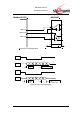
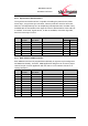
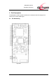
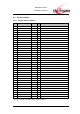
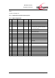
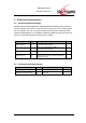
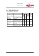
Table Of Contents
- Introduction
- Block Diagram
- Application Interface
- Pin Description
- Electrical Characteristics
- Mechanical Characteristics
- Approvals/Certifications
- Related Documents
- Ordering Information
- History

BlueMod+C11/G2
Hardware Reference
www.stollmann.de Page 12 of 42
3.5 GPIO Interface
All user signals, except for EXT-RES#, which is routed via an Schmitt Trigger gate,
are connected directly to port pins of the ATMEL AT91SAM7S256 CPU. Except for
USB signals DP, DM and GPIO(4), no additional pull-up or down resistors are im-
plemented, so that the I/O characteristics of the ATMEL CPU apply. These are
3V3 logic 5V tolerant
V
IL
max = 0.8V, V
IH
min = 2.0V, V
IH
max = 5.5V
V
OH
min = VCC – 0.4V @ I
O
= 8mA, V
OL
< 0.4V @ I
O
= 8mA
LED’s can be driven directly on specific GPIO lines when I
o
stays below 8mA
All current consumption data in this document are given with I
O
(GPIO) = 0mA
See chapter 5 Electrical Characteristics for detailed information.
All I/O signals except USB, GPIO(4) and JTAG are connected directly from the
AT91SAM7S pins to the user accessible stamp pins. Therefore, the electrical
characteristics of the I/O pins are programmable in regard to direction, pull-up
resistor, function, push-pull or open drain. Please see specific application soft-
ware documentation for details. After reset, all GPIOs have pull-ups activated.
GPIO10, GPIO8 and TXD have 50kR to 300kR pull-ups, all other I/Os have 5kR
to 20kR pull-ups
3.6 Alternate GPIO/IO Functions
Application specifically dedicated GPIO or IO pins can be programmed to alternative
functionalities. Then pin functionality and direction are fixed for the activated function
block. Many GPIOs are used by the SPP application. See chapter SPP Configura-
tion. Probably some of them can be released for use by other function blocks. Co-
functionality of blocks has to be carefully considered, because pin multiplexing pos-
sibilities are fixed by the ATMEL AT91SAM7S CPU and using a function block often
causes that other function blocks can’t be used at the same time. Please refer to the
ATMEL data sheet AT91SAM7Sxxx Rev. F for complete information. The possibili-
ties depicted in the following chapters are a subset only.
The following function blocks may be usable on the BlueMod+C11/G2:
3.6.1 Master/Slave SPI Interface
Pin #
GPIO#
IO Name
Alternative
Signal Name
Description
Direction
Master
Slave
A5
GPIO1
MISO
Master In Slave Out
IN
OUT
A4
GPIO0
MOSI
Master Out Slave In
OUT
IN
A3
GPIO3
SPCK
Serial Clock
OUT
IN
A6
GPIO2
NPCS0
Peripheral. Chip Select
OUT
IN
Clock polarity and phase are programmable. The chip select signal is low active.