
Technical Manual

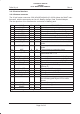
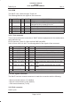
Table Of Contents
- GENERAL INDEX
- 1 INTRODUCTION
- 2 MECHANICAL VIEW
- 3 TECHNICAL SPECIFICATIONS
- 3.1 Operating frequencies
- 3.2 Transmitter output power
- 3.3 Reference sensitivity
- 3.4 Antenna
- 3.5 Audio characteristics
- 3.5.1 Microphone
- 3.5.1.1 Microphone sensitivity
- 3.5.1.1.1 Microphone electric level
- 3.5.1.1.2 Microphone distorsion
- 3.5.1.2 Buzzer
- 3.5.1.2.1 Acoustic pressure of the buzzer
- 3.5.1.3 Vibrator
- 3.6 Device voltage supply
- 3.6.1 Power consumption
- 3.7 Keypad
- 3.8 Display
- 3.9 Data service
- 3.10 Software functionality and user interface
- 3.11 Electrical interface
- 3.11.1 Bottom connector
- 3.11.2 SIM
- 3.11.3 Test connector
- 3.11.4 RF signals connector
- 3.11.5 DAI connector
- 3.12 Physical characteristics
- 3.13 Dimensions
- 3.14 Weight
- 3.15 Figures
- 4 LIST OF MODIFICATIONS
- 5 BLOCK DIAGRAMS
- 6 ELECTRIC DIAGRAMS
- CS710c GSM Radio board page 1/3
- CS710c GSM Radio board page 2/3
- CS710c GSM Radio board page 3/3
- CS680b Microphone Input & GS codec 1/15
- CS680b GSM uP, memory & RTC 2/15
- CS680b GAIM 3/15
- CS680b Power Supply & Reset 4/15
- CS680b Keyboard & display connectors 5/15
- CS680b SIM interface 6/15
- CS680b GSM radio connector 7/15
- CS680b Battery charge 8/15
- CS680b Bottom connector 9/15
- CS680b GS uP 10/15
- CS680b GS uP 11/15
- CS680b GUM ASIC 12/15
- CS680b GS vocoder 13/15
- CS680b BB2 ASIC 14/15
- CS680b GS radio connector 15/15
- CS661c Rx car kit switch & RF ampl. 1/9
- CS661c Rx phase shifter, IF filter, AGC 2/9
- CS661c Tx AGC and IF filter 3/9
- CS661c Tx upconverter, driver 4/9
- CS661c Tx power amplif, ADC multiplexer 5/9
- CS661c RF synthesizer 6/9
- CS661c General Power Supply 7/9
- CS661c Tx drv. & power ampl. p.supp 8/9
- CS661c BB connector & GSM ant. switch 9/9
- CS760 Optical Sensor Board 1/1
- 7 PARTS LIST
- 8 PHOTOS AND ASSEMBLIES
- 9 USER GUIDE

Rev. 1Telital S.p.A.
TECHNICAL MANUAL
GS/GSM
DUAL MODE USER TERMINAL
Page 9 of 13
3.11.2 SIM
The DMUT uses a SIM card type ”PLUG–IN”.
The following table list the signals of SIM connector.
PIN
NAME A/D IN/OUT DESCRIPTION
1 C1,CCVCC A IN % !#&
2 C2, RST D OUT "$ #
& " "!
3 C3,CCLK D OUT !# # " "
4 C5,GND A IN #" # " "
5 C6,NC ––– ––– " "
6 C7,I/O D IN/OUT #"#"#" " "
3.11.3 Test connector
This connector allows the connection of DMUT with test equipments for the maintenance,
and production test.
ELCO connector Torson 2 x 5pins vertical SMD low profile.
P/N 23–5016–2005–10–081. The following table list the signals of test connector.
PIN
NOME A/D IN/OUT DESCRIPTION
1 WAKEUP D IN Signal for remote power on.
2 RST D IN Reset
3 TXD1 D OUT Data transmission from 80386 serial line #1
4 RXD1 D IN Data reception to 80386 serial line #1
5 GND A –– Ground
6 DWLD D IN Download in G* mode enabled
7 INT3 D IN Not used
8 GSM_TX_DATA D OUT Data transmission and monitor line in GSM
mode
9 GSM_RX_DATA D IN Data reception and monitor line in GSM
mode
10 +VBATT A –– Positive 7.4V power supply
Legenda: A: Analogico; D: Digitale 0 3V CMOS
3.11.4 RF signals connector
The DMUT has three coaxial connectors to made the connection with the following:
– Band L external antenna (Tx satellite)
– Band S external antenna (Rx satellite)
– GSM external antenna (Tx /Rx)
3.11.5 DAI connector
Pads on pcb.