
User's Manual

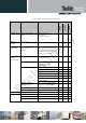
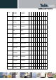
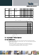
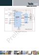
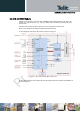
Table Of Contents
- 1 Introduction
- 2 M.2 Overview
- 3 M.2 Module Interface Details
- 3.1 USB 2.0 High-Speed – IPC Interface
- 3.2 (U)SIM Interface
- 3.3 GNSS Interface
- 3.4 System Control Interface
- 3.5 Tunable Antenna Control Interface
- 3.6 In-Device Coexistence Interface
- 3.7 Power Supply Interface
- 3.8 Trace & Debug Interface
- 3.9 Configuration Pins
- 3.10 Reserved Pins
- 3.11 No Connect Pins
- 3.12 Antenna Interface
- 4 Development Tools
- 5 Windows Software Components
- 6 Modem Configuration on Linux Based PC
- 7 Operating Environment
- 8 Power Delivery Requirements
- 9 Other Information
- 10 WWAN Card Type 3042-S3-B
- 11 Safety Recommendations
- 12 Conformity assessment issues
- 13 FCC/IC Regulatory notices
- 14 Document History

xN930 M.2 Hardware User Guide
1VV0301078 Rev.6 – 2013-11-12
028 XXVIII
703 MHz -
748 MHz
758 MHz -
803 MHz
029 XXIX
1850 MHz -
1910 MHz
or
1710 MHz -
1755 MHz
716 MHz -
728 MHz
001 I
1920 MHz -
1980 MHz
2110 MHz -
2170 MHz
Table 3. M.2 Module - Data Services
Data Service
M.2 module
HN930
LN930-AP
LN930
GPRS Class 33: DL 85.6 kbps, UL 85.6 kbps
x
-
x
EDGE Class 33: DL 236.8 kbps, UL 236.8 kbps
x
-
x
WCDMA: DL 384 kbps, UL 384 kbps
x
x
x
HSPA+: DL 21 Mbps, UL 5.7 Mbps
x
x
x
HSPA+: DL 42 Mbps, UL 5.7 Mbps
-
x
x
LTE FDD: DL: 100 Mbps, UL 50 Mbps
-
x
x
2.2
M.2 Module – Block Diagrams
2.2.1
M.2 HN930 Module
The M.2 HSPA+ module is Intel’s Next Generation Form Factor design based on Intel’s
XMM™6260 modem platform. The M.2 HSPA+ card is a dual-mode (UMTS/GSM) 3GPP
release 7 HSPA+ modem.
The M.2 HSPA+ module includes support at the 75 pin application interface for
M.2 Control, USB 2.0 HS, GNSS, and USIM. Antenna Tuning is not supported.
A block diagram of the M.2 HSPA+ module is shown in
Figure 1
.
Reproduction forbidden without written authorization from Telit Communications S.p.A. - All Rights Reserved. Page 17 of 77