
User Guide


LM960 HW Design Guide
1VV0301485 Rev. 15 Page 86 of 88 2020-08-13
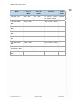
15. DOCUMENT HISTORY
Revision
Date
Changes
0 2018-02-09 First Draft
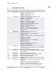
1 2018-05-30 Updated 1.5 Related documents
Updated 3.3 Pin Layout
Updated 4.2 Power Consumption
Updated 6 Digital Section
2 2018-07-05 Updated 2.2.1 RF Bands per Regional Variant
Updated 2.6 Tx output power
Updated 2.7 Rx sensitivity
Updated 2.8.2 Weight
Updated 4.2 Current Consumption
Updated 6.6.1 USB Block Diagram
Updated 6.6.2 PCIe Block Diagram Updated
Deleted 6.5.4 PCIE_WAKE_N
Updated 7.1 Antenna Requirements
Updated 8.3 Drawing
Updated 11.5 FCC/IC Regulatory notices
Updated 13 Reference Table of RF Bands
Characteristic
3
2018
-
12
-
06
Updated
2 General
P
roduct Description
4 2019-03-15 Updated 3.1 Pin-out
Changed PCIE_RESET_N pin description
6 Digital Section
Changed description about setting GPIO as specific
function.
Updated 6.2 Power ON
Updated 6.3 Power Off
Fast Shutdown Trigger: Low Edge Trigger
Updated 6.4 Reset
Added 6.5 Dying Gasp
Dying Gasp Trigger: Low Edge Trigger
Added 6.6.5.3 Dedicated I/O
Added 6.6.4.2 WAN_LED_N
5 2019-04-17 Updated 6.3.2 Fast Shutdown Timing and 2.2.1 RF Bands
per Regional Variant, LM960A18 Variant introduced,
various editorial changes
6
2019
-
06
-
04
Moisture Sensitivity Level paragraph added
7 2019-07-17 Band and CA combo list updated, minor editorial changes
and corrections
8
2020
-
01
-
21
Moisture Sensitivity Level corrected
9 2020-01-31 Antenna port paragraph corrected (band 43 added)
10
2020
-
02
-
05
Moisture Sensitivity Declaration removed
11 2020-02-12 PCIe bus references removed
12 2020-04-01 Updated 2.7 RX Sensitivity, added lte fdd band43
senstivity level
13 2020-05-29 Updated 2.2.1.3 2 LM960A9-P RF Bands and Carrier
Aggregation
Updated 2.4 Main Features, Added LM960A9-P
Updated 2.8.2 Weihgt, Added LM960A-P
Udated 7.1 Antenna requirement, Added LM960A9-P
Udated 7.5 Antenna connection, Added LM960A9-P