
User Guide


LM960 HW Design Guide
1VV0301485 Rev. 15 Page 38 of 88 2020-08-13
The PCB traces connecting the switching output to the inductor and the switching
diode must be kept as short as possible by placing the inductor and the diode very
close to the power switching IC (only for the switching power supply). This is done
to reduce the radiated field (noise) at the switching frequency (usually 100-
500 kHz).
Use a good common ground plane.
Place the power supply on the board in a way to guarantee that the high current
return paths in the ground plane do not overlap any noise sensitive circuitry, such
as the microphone amplifier/buffer or earphone amplifier.
The power supply input cables must be kept separate from noise sensitive lines,
such as microphone/earphone cables.
RTC
The RTC within the LM960 module does not have a dedicated RTC supply pin. The RTC
block is supplied by the VBATT supply.
If VBATT power is removed, RTC is not maintained so if maintaining an internal RTC is
needed, VBATT must be supplied continuously.
Reference Voltage
1.8V regulated power supply output is provided as the reference voltage to a host board.
This output is active when the module is ON and goes OFF when the module is shut
down.
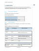
This table lists the VREG_L6_1P8 signal of LM960.
LM960 Reference Voltage
PIN Signal I/O Function Type Comment
28 VREG_L6_1P8 O Reference Voltage power 1.8V
Internal LDO for GNSS bias
The LDO for GNSS bias is applied inside the LM960 model.
The voltage supply come from LM960’s LDO to GNSS active antenna.
This table lists the LDO for GNSS bias of LM960.
LM960 Reference Voltage when VBATT is 3.3