
User's Guide


LE910Cx HW User Guide
Doc#: 1VV0301298
Rev. 13.0 Page 121 of 124 2019-07-15
Revision
Date
Changes
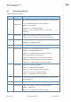
5
2018-09-16
Section 14 – Adding Antenna gain and FCC ID & IC numbers
for LE910C1/C4 NF.
Section 5.2 – Fixed typo related to power up timing.
4
2018-08-20
Table 1 & 4 - Added LE910C4-EU variant
Section 2.3 – Updated SIM interface max speed
Declared HSIC interface as optional throughout the document
Section 2.6.2 – Updated RF frequency table
Section 6.2 – Added clarification related to DRX and CFUN=5
Section 8.1 - Corrected Typo related to USB_VBUS pad
number
Section 8.4.1- Clarified note about DTR pin
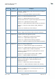
3
2018-07-18
Section 2.8.1 - Fixed typo related to module size
General - Align cross reference links across the document
2
2018-06-14
Template update and pagination update
Section 1.5 – Updated AT Command UG reference
Section 2.6.1 - Updated Band support table
Section 6.3.2 - Updated Thermal design guidelines
Section 8.3 - Removed “optional” term from Ethernet interface
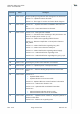
1.13
2018-05-17
Added new variant LE910C1-NF
Section 2.6.1 - Added band 66 support for LE910Cx-NF
Section 2.6.2 - Added band 66 and band 71 to frequency table
Section 3.1 - Updated value of SIM internal pullup
Section 8.3 – added clarification regarding Ethernet control
interface logic levels
Section 8.5.4 – Removed note related to WIFI_SDRST
Section 9.7 - Updated GNSS characteristics
1.12
2018-03-18
Replaced LE910C1 with LE910Cx throughout the document
Section 2.6.1 and Table 1 - Added LE910C1-EU and
LE910C4-NF variants
Section 8.7 – Added notes related to GPIO pullups
Section 10.7.2 - Added clarification related to flux cleaning
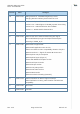
1.11
2018-02-22
Section 5.3.2 – Updated section name
Section 5.4 – Added section for clarifying power down and
power off procedures
Section 8.6.1 – Update for PCM slave mode