
User's Guide

LE910Cx HW User Guide
Doc#: 1VV0301298
Rev. 13.0 Page 53 of 124 2019-06-07
6. Power Supply
The power supply circuitry and board layout are very important parts of the full product
design, with critical impact on the overall product performance. Read the following
requirements and guidelines carefully to ensure a good and proper design.
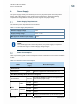
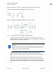
Power Supply Requirements
The LE910Cx power requirements are as follows:
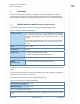
Table 17: Power Supply Requirements
Nominal supply voltage 3.8V
Supply voltage range 3.4V – 4.2V
Max ripple on module input supply 30 mV
NOTE:
For PTCRB approval on the final products, the power supply is required to
be within the range of “Normal Supply voltage ranger”.
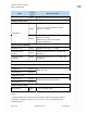
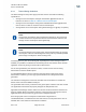
Power Consumption
Table 18 provides typical current consumption values of LE910Cx for the various available
modes.
Table 18: LE910Cx Current Consumption
Mode
Average
(Typ.)
Mode Description
Switched Off
Switched off 25µA Module supplied but switched Off (RTC On)
Idle Mode (Standby Mode; No Call in Progress)
AT+CFUN=4 10.0 mA
Tx and Rx disabled; module is not registered on
the network (Flight mode)
DRX
AT+CFUN=5
GSM
2.4 mA DRx2
1.9 mA DRx5
WCDMA
1.9 mA DRx7
1.7 mA DRx8
LTE 2.1mA Paging cycle #128 frames (1.28 sec DRx cycle)