
User's Guide

LE910Cx HW User Guide
Doc#: 1VV0301298
Rev. 13.0 Page 28 of 124 2019-06-07
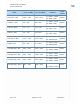
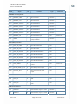
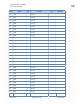
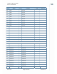
PAD Signal I/O Function Type Comment
D7 ADC_IN3 AI
Analog/Digital Converter Input
3
Analog
SGMII Interface
E4 SGMII_RX_P AI SGMII receive – plus PHY
F4 SGMII_RX_M AI SGMII receive – minus PHY
D5 SGMII_TX_P AO SGMII transmit – plus PHY
D6 SGMII_TX_M AO SGMII transmit - minus PHY
HSIC Interface
A12 HSIC_DATA I/O
High-speed inter-chip interface
- data
1.2V Optional
A11 HSIC_STB I/O
High-speed inter-chip interface
- strobe
1.2V Optional
I2C Interface
B11 I2C_SCL I/O I2C clock 1.8V
Internally PU
2.2kΩ to 1.8V
B10 I2C_SDA I/O I2C Data 1.8V
Internally PU
2.2kΩ to 1.8V
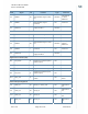
Power Supply
M1 VBATT -
Main Power Supply (Digital
Section)
Power
M2 VBATT -
Main Power Supply (Digital
Section)
Power
N1 VBATT_PA -
Main Power Supply (RF
Section)
Power
N2 VBATT_PA -
Main Power Supply (RF
Section)
Power
P1 VBATT_PA -
Main Power Supply (RF
Section)
Power
P2 VBATT_PA -
Main Power Supply (RF
Section)
Power
A2 GND - Ground
B13 GND Ground
D4 GND - Ground