
Hardware Manual
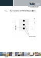


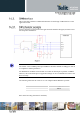

This section deals with the recommended schematics for the design of SIM interfaces on the
application boards.
Figure 1 illustrates in particular how the application side should be designed, and what values
the components should have.
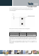
NOTE FOR R1:
The resistor value on SIMIO pulled up to SIMVCC should be defined accordingly in order to
be compliant to 3GPP specification.
For HE910-EUG V2/NAG V2/EU V2/NA V2 contain an internal pull-up resistor on SIMIO.
However, the un-mounted option in application design can be recommended in order to tune
R1 if necessary.
The following Table lists the values of C1 to be adopted with the HE910 V2 product:
Product P/N
C1 range (nF)
HE910-EUG/NAG V2
100 nF
HE910-EU/NA V2
Refer to the following document for the detail;