
User's Manual


GL865 Hardware User Guide
1vv0300910 Rev.1 – 2011-07-22
Reproduction forbidden without Telit Communications S.p.A. written authorization - All Rights Reserved
page 34 of 79
7.3. PCB Guidelines in case of FCC certification
In the case FCC certification is required for an application using
GL865, according to FCC KDB 996369 for modular approval requirements,
the transmission line has to be similar to that implemented on GL865
interface board and described in the following chapter.
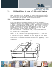
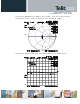
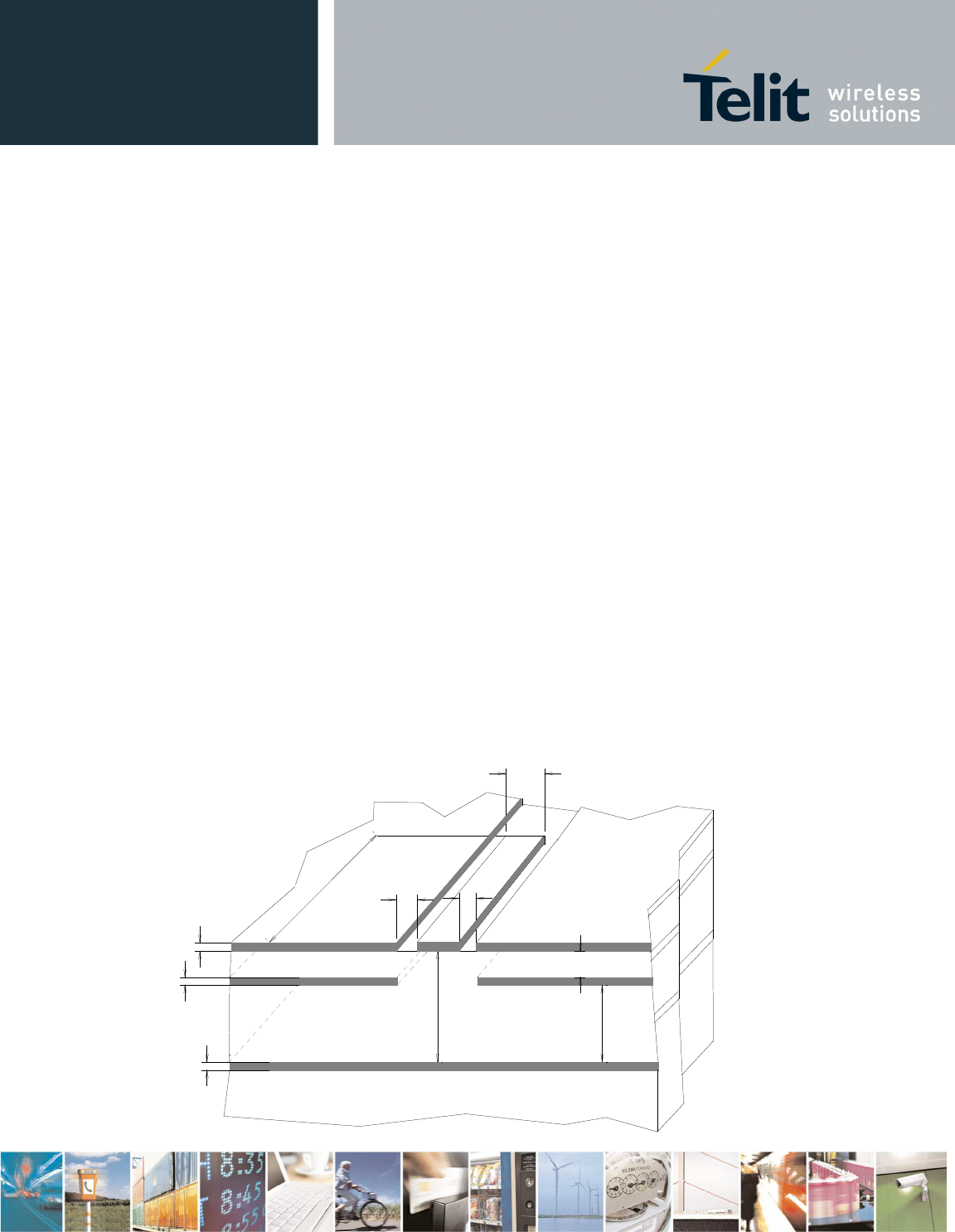
7.3.1. Transmission line design
During the design of the GL865 interface board, the placement of
components has been chosen properly, in order to keep the line length
as short as possible, thus leading to lowest power losses possible. A
Grounded Coplanar Waveguide (G-CPW) line has been chosen, since this
kind of transmission line ensures good impedance control and can be
implemented in an outer PCB layer as needed in this case. A SMA
female connector has been used to feed the line.
The interface board is realized on a FR4, 4-layers PCB. Substrate
material is characterized by relative permittivity ε
r
= 4.6 ± 0.4 @ 1
GHz, TanD= 0.019 ÷ 0.026 @ 1 GHz.
A characteristic impedance of nearly 50 Ω is achieved using trace
width = 1.1 mm, clearance from coplanar ground plane = 0.3 mm each
side. The line uses reference ground plane on layer 3, while copper
is removed from layer 2 underneath the line. Height of trace above
ground plane is 1.335 mm. Calculated characteristic impedance is 51.6
Ω, estimated line loss is less than 0.1 dB. The line geometry is
shown below:
0.3 mm
0
.
0
3
5
m
m
0.3 mm
6
.
2
m
m
FR4
0
.
0
3
5
m
m
0
.
0
3
5
m
m
1
.
3
3
5
m
m
0
.
2
m
m
1
.
1
m
m
L3
L2
L1
1.1 mm