
User's Manual

GL865 Hardware User Guide
1vv0300910 Rev.1 – 2011-07-22
Reproduction forbidden without Telit Communications S.p.A. written authorization - All Rights Reserved
page 30 of 79
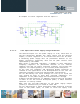
6.3.3. Power Supply PCB layout Guidelines
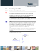
As seen on the electrical design guidelines the power supply
shall have a low ESR capacitor on the output to cut the current
peaks and a protection diode on the input to protect the supply
from spikes and polarity inversion. The placement of these
components is crucial for the correct working of the circuitry.
A misplaced component can be useless or can even decrease the
power supply performances.
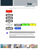
The Bypass low ESR capacitor must be placed close to the Telit
GL865 power input pads or in the case the power supply is a
switching type it can be placed close to the inductor to cut the
ripple provided the PCB trace from the capacitor to the GL865 is
wide enough to ensure a dropless connection even during the 2A
current peaks.
The protection diode must be placed close to the input connector
where the power source is drained.
The PCB traces from the input connector to the power regulator
IC must be wide enough to ensure no voltage drops occur when the
2A current peaks are absorbed. Note that this is not made in
order to save power loss but especially to avoid the voltage
drops on the power line at the current peaks frequency of 216 Hz
that will reflect on all the components connected to that supply,
introducing the noise floor at the burst base frequency. For
this reason while a voltage drop of 300-400 mV may be acceptable
from the power loss point of view, the same voltage drop may not
be acceptable from the noise point of view. If your application
doesn't have audio interface but only uses the data feature of
the Telit GL865, then this noise is not so disturbing and power
supply layout design can be more forgiving.
The PCB traces to the GL865 and the Bypass capacitor must be
wide enough to ensure no significant voltage drops occur when
the 2A current peaks are absorbed. This is for the same reason
as previous point. Try to keep this trace as short as possible.
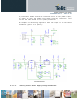
The PCB traces connecting the Switching output to the inductor
and the switching diode must be kept as short as possible by
placing the inductor and the diode very close to the power
switching IC (only for switching power supply). This is done in
order to reduce the radiated field (noise) at the switching
frequency (100-500 kHz usually).
The use of a good common ground plane is suggested.
The placement of the power supply on the board should be done in
such a way to guarantee that the high current return paths in
the ground plane are not overlapped to any noise sensitive
circuitry as the microphone amplifier/buffer or earphone
amplifier.