
User's Manual
GL865 Hardware User Guide
1vv0300910 Rev.1 – 2011-07-22
Reproduction forbidden without Telit Communications S.p.A. written authorization - All Rights Reserved
page 24 of 79
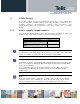
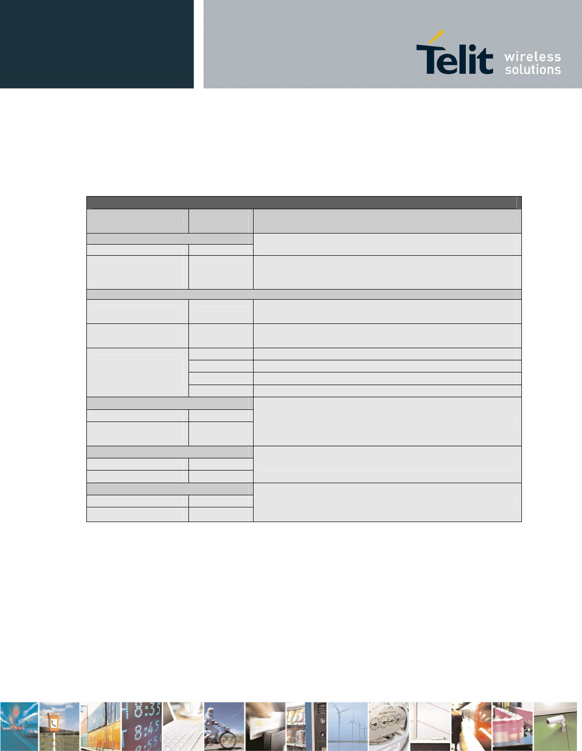
6.2. Power Consumption
The GL865 power consumptions are:
GL 865
Mode
Average
(mA)
Mode description
SWITCHED OFF
Module power supplied only on VBATT_PA pin,
the VBATT pin is not power supplied.
Switched Off <5uA
Switched Off
with
AT#SYSHALT
<650uA
Module power supplied on VBATT_PA pin and
VBATT pin, the at command
AT#SYSHALT
is
applied.
IDLE mode
AT+CFUN=1
21,0
Normal mode: full functionality of the
module
AT+CFUN=4
18,0
Disabled TX and RX; module is not
registered on the network
AT+CFUN=0 or
=5
3,9
Paging Multiframe 2
2,5
Paging Multiframe 3
2,4
Paging Multiframe 4
1,5
Paging Multiframe 9
CSD TX and RX mode
GSM VOICE CALL
GSM900 CSD PL5
230
DCS1800 CSD
PL0
180
GPRS (class 8) 1TX
GPRS Sending data mode GSM900 PL5
225
DCS1800 PL0
175
GPRS (class 10) 2TX
GPRS Sending data mode
GSM900 PL5 360
DCS1800 PL0 300
The GSM system is made in a way that the RF transmission is
not continuous, else it is packed into bursts at a base
frequency of about 216 Hz, and the relative current peaks
can be as high as about 2A. Therefore the power supply has
to be designed in order to withstand with these current
peaks without big voltage drops; this means that both the
electrical design and the board layout must be designed for
this current flow.
If the layout of the PCB is not well designed a strong
noise floor is generated on the ground and the supply; this
will reflect on all the audio paths producing an audible
annoying noise at 216 Hz; if the voltage drop during the
peak current absorption is too much, then the device may
even shutdown as a consequence of the supply voltage drop.