
User's Manual
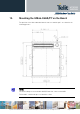
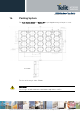
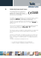

Table Of Contents
- GC864 Hardware User Guide
- APPLICABILITY TABLE
- 1. Introduction
- 2. Overview
- 3. GC864 Mechanical Dimensions
- 4. GC864-QUAD/PY Module Connections
- 5. Hardware Commands
- 6. Power Supply
- 7. Antenna
- 8. Logic Level Specifications
- 9. Serial Ports
- 10. Audio Section Overview
- 11. General Purpose I/O
- 11.1. GPIO Logic Levels
- 11.2. Using a GPIO Pad as INPUT
- 11.3. Using a GPIO Pad as OUTPUT
- 11.4. Using the RF Transmission Control GPIO4
- 11.5. Using the RFTXMON Output GPIO5
- 11.6. Using the Alarm Output GPIO6
- 11.7. Using the Buzzer Output GPIO7
- 11.8. Magnetic Buzzer Concepts
- 11.9. Using the Temperature Monitor Function
- 11.10. Indication of Network Service Availability
- 11.11. RTC Bypass Out
- 11.12. VAUX1 Power Output
- 12. DAC and ADC Section
- 13. Mounting the GC864-QUAD/PY on the Board
- 14. Packing System
- Conformity Assessment Issues

GC864 Hardware User Guide
1vv0300733 Rev.12 – 2009-06-04
13.1.1. Debug of the GC864-QUAD/PY in Production
To test and debug the mounting of the GC864, we strongly recommend to foreseen
test pads on the host PCB, in order to check the connection between the GC864-
QUAD/PY itself and the application and to test the performance of the module
connecting it with an external computer. Depending by the customer application,
these pads include, but are not limited to the following signals:
• TXD
• RXD
• ON/OFF
• RESET
• GND
• VBATT
• TX_TRACE
• RX_TRACE
• PWRMON
Reproduction forbidden without Telit Communications S.p.A’s. written authorization - All Rights Reserved. Page 64 of 69