QPHY-DDR4 Operator’s Manual Revision A – June, 2014 Relating to the Following Release Versions: • Software Version Rev. 7.4 • DDR4 Script Rev. 7.4 • Style Sheet Rev. 1.
700 Chestnut Ridge Road Chestnut Ridge, NY, 10977-6499 Tel: (845) 425-2000, Fax: (845) 578 5985 teledynelecroy.com © 2014 by Teledyne LeCroy. All rights reserved. Teledyne LeCroy and other product or brand names are trademarks or requested trademarks of their respective holders. Information in this publication supersedes all earlier versions. Specifications are subject to change without notice.
QPHY-DDR4 Software Option TABLE OF CONTENTS Introduction to Qualiphy DDR4 ................................................................................................6 Required Equipment ..................................................................................................................................... 6 Using Qualiphy DDR4 ...............................................................................................................7 QualiPHY Compliance Test Platform .................
TABLE OF FIGURES Figure 1 - Report menu in QualiPHY General Setup................................................................................ 8 Figure 2 - The Test Report includes a summary table with links to the detailed test results ............. 9 Figure 3 - QualiPHY main menu and compliance test Standard selection menu ............................... 11 Figure 4 - QualiPHY configuration selection menu ...............................................................................
QPHY-DDR4 Software Option Figure 53 - Oscilloscope Configuration after the tDQSS test ............................................................... 62 Figure 54 – tDQSS Results ....................................................................................................................... 63 Figure 55 - Oscilloscope Configuration after the tDQSH test .............................................................. 64 Figure 56 – tDQSH/tDQSL Results ....................................................
Introduction to Qualiphy DDR4 QPHY-DDR4 is an automated test package performing all of the real time oscilloscope in accordance with JEDEC Standard No. JESD79-4. The standard is available on jedec.org. The software can be run on any Teledyne LeCroy Zi Series oscilloscope with at least 8 GHz bandwidth. The oscilloscope must also be equipped with the QPHY-DDR4 and SDAIII options. Required Equipment • Real time Teledyne LeCroy Oscilloscope with at least 8 GHz bandwidth.
QPHY-DDR4 Software Option Using Qualiphy DDR4 QualiPHY DDR4 guides the user, step-by-step, through each of the tests in conformance with the JEDEC DDR4 specification: JESD79-4. To do this, the user must set up a test session. Before beginning testing, users choose the test configuration they wish to run. There are seven preloaded test configurations.
QualiPHY Compliance Test Platform QualiPHY is Teledyne LeCroy’s compliance test framework which leads the user through the compliance tests. QualiPHY displays connection diagrams to ensure tests run properly, automates the oscilloscope setup, and generates complete, detailed reports. The QualiPHY software application automates the test and report generation.
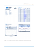
QPHY-DDR4 Software Option Figure 2 - The Test Report includes a summary table with links to the detailed test results 924291 Rev A 9
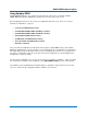
Oscilloscope Option Key Installation The required option keys must be purchased to enable the QPHY-DDR4 compliance tests. If you do not have the required option keys already call Teledyne LeCroy Customer Support to place an order and receive the codes. Enter the key and enable the purchased option as follows: 1. From the oscilloscope menu select Utilities Utilities Setup... 2. Select the Options tab and click the Add Key button. 3. Enter the Key Code using the on-screen keyboard. 4.
QPHY-DDR4 Software Option QualiPHY tests the oscilloscope connection after clicking the Start button. The system prompts you if there is a connection problem. QualiPHY’s Scope Selector function can also be used to verify the connection. Please refer to the QualiPHY Operator’s Manual for explanations on how to use Scope Selector and other QualiPHY functions. Accessing the QPHY-DDR4 Software using QualiPHY This topic provides a basic overview of QualiPHY’s capabilities.
Figure 4 - QualiPHY configuration selection menu 6. Click Start. 7. Follow the pop-up window prompts.
QPHY-DDR4 Software Option Customizing QualiPHY The predefined configurations in the Configuration screen cannot be modified. However, you can create your own test configurations by copying one of the standard test configurations and making modifications. A description of the test is also shown in the description field when selected.
Creating Custom Configurations Beginning with any of the pre-loaded configurations, 1. Click on the Test Selector tab to change what tests you would like to be included in your new configuration. 2. Click on the Variable Setup tab to change the variables for your new configuration. 3. Click on the Limits tab to change which limit set should be used for your new configuration •See QualiPHY Manual for more information 4.
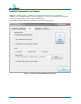
QPHY-DDR4 Software Option Figure 6 - Variable Setup and Limits Manager windows 924291 Rev A 15
QPHY-DDR4 OPERATION After pressing Start in the QualiPHY menu, the software instructs how to set up the test using pop-up connection diagrams and dialog boxes. QualiPHY also instructs how to properly configure the Device Under Test (DUT) to change test signal modes (when necessary).
QPHY-DDR4 Software Option QPHY-DDR4 Measurement Preparation Deskewing the Probes For DDR measurements it is crucial to make sure the probes are properly deskewed before running QPHY-DDR4 to ensure proper signal timing. Ideally, when deskewing the same settings should be used as when QualiPHY is acquiring the signals for analysis. This will ensure that the channels are deskewed using the same setup as when running conformance tests. Deskew values are saved and stored by QPHY at the beginning of each run.
Once everything is properly set up the oscilloscope display should look similar to the figure below. If there was no propagation delay due to the probe, and no internal oscilloscope channel propagation delay, the 50% trigger level would be in the middle of the oscilloscope grid. The channel’s deskew value shall be adjusted so that the 50% rising edge point is centered in time, as shown below. From the channel setup dialog, enable Sinx/x interpolation and set the averaging to 50 sweeps.
QPHY-DDR4 Software Option Connecting the Probes Determining Signals to Access The required signals to probe depend up on which tests are being run in QPHY-DDR4. The tests are broken up into different “Probe Setups” to allow the user to easily see which signals are required for a particular test. You can view each of the probe setups in the Test Selector tab.
R/W Burst Generation QPHY-DDR4 recommends to have a minimum of 10 R and 10 W bursts during each acquisition but for greater statistical significance it is encouraged to have more. Programs which can communicate with the DRAM and controller are widely available online. One example is Memtest86+ which is available for download from memtest.org. When using Memtest it is recommended to use test mode 7, which will randomly generate both R and W bursts.
QPHY-DDR4 Software Option Initial Signal Checking Before running QPHY-DDR4 the user should have a quick look at their signals to verify that they make sense. This section covers some of the basic things which should be verified by the operator before running QPHY-DDR4. Expected Channels By default QPHY-DDR4 expects to see the clock (CK) on CH1, DQS on CH2 and DQ on CH3. This is what is shown in the connection diagram. The Channel Index variable can always be used to modify any of these channels.
Presence of R/W Burst The operator should do a quick check to make sure their device is outputting the expected bursts. As a general rule of thumb, during a R burst DQ and DQS should be in phase and during a W burst DQ and DQS should be a quarter cycle out of phase. Additionally, the signal amplitude can be used to determine the presence of R and W bursts. If probing at the memory R bursts will have a larger amplitude than W bursts.
QPHY-DDR4 Software Option QPHY-DDR4 Test Configurations Configurations include variable settings and limit sets as well, not just test selections. See the QPHYDDR4 Variables section for a description of each variable value and its default value. 1) Clock tests DDR4-1600 (1 Probe) This configuration will run all of the clock tests and requires 1 probe to be connected to the differential clock. All of the variables are set to their default settings. The limit set in use is DDR4-1600.
QPHY-DDR4 Variables Custom Speed Grade in MT/s This variable allows the user to define a custom speed grade to be used. This speed grade is used to set the oscilloscope timebase and sampling rate, see Clock Period Per Screen Division for more information. The default value for this variable is 0. Using the default value, QPHY will read the speed grade from the selected limit set. Waveform Path This variable allows the user to specify the path on the oscilloscope to save and recall waveforms.
QPHY-DDR4 Software Option DQS_c Signal Name This variable allows the user to assign a name to the DQS_c signal to appear in the test report and screenshots. The default signal name is DQS0_c. ADD/CTRL Signal Name This variable allows the user to assign a name to the ADD/CTRL signal to appear in the test report and screenshots. The default signal name is A0. CK_t Signal Name This variable allows the user to assign a name to the CK_t signal to appear in the test report and screenshots.
Demo Settings These variables must be adjusted if the user wishes to run QPHY using saved waveforms. Use Stored Waveforms When enabled QPHY will run using previously stored waveforms. The waveforms will be recalled using the defined Waveform Path. The default value is No. Recalled Waveform File Index (5 digits) QPHY will recall the saved waveform file using the defined 5 digit index of the file. The default value is 00000.
QPHY-DDR4 Software Option Advanced Settings - Custom Levels Standard, Custom or Auto Levels This variable allows the user to use either Standard, Custom, or Auto Levels. Standard uses the levels defined by the JEDEC specification. Custom uses the VIH/VIL AC/DC levels defined by the custom levels variables. Auto uses the levels QPHY automatically calculates from the top and base of the acquired waveform. The VIH and VIL levels are calculated using AC120.
Probe Setup: CKdiff These variables control the probe setup for the configuration using a differential clock (CK) only. Jitter BER Level This variable defines the BER level which will be used by SDA during the tJIT(per) and tJIT(cc) tests. The default value is -12. CAS Latency, CAS Write Latency, Speed Bin These variables are used to define the tCK(avg) limits as defined in tables 80-83 in JESD79-4. These variables are only used by QPHY when Speed Bin Parameters Automatic Selection is set to No.
QPHY-DDR4 Software Option QPHY-DDR4 Test Descriptions Clock Tests (Ck Diff) There are 8 tests run in this group. The tests that are run are: 1. tCK(avg), tCK(abs) 2. tCH(avg), tCL(avg), tCH(abs), tCL(abs) 3. tJIT(duty) 4. tJIT(per)_total 5. tJIT(per)_dj 6. tJIT(cc)_total 7. tJIT(cc)_dj 8. tERR(n per) Each of these tests is described in detail below.
After the completion of the tCK, tCH, tCL, and tJIT(duty) tests the oscilloscope is in the following configuration: Figure 14 - Oscilloscope Configuration after tCK, tCH, tCL and tJIT(duty) Tests Shown on this screen: • Z1 is a zoom of the differential clock signal 30 924291 Rev A
QPHY-DDR4 Software Option Figure 15 - tCK, tCH, tCL and tJIT(duty) Results In the Measure section: • tCK rise (P1) is the period measurement at Vref (0 mV) of Z1 (differential clock signal) on only the rising edges. The mean value is the measured value for tCK(avg), rise. The minimum value is the measured value for tCK(abs), rise, min reported in mtCK(avg). The maximum value is the measured value for tCK(abs), rise, max reported in mtCK(avg).
• tJIT(CL) (P6) subtracts the mean of P4 (tCL(avg)) from all of the tCL values. The minimum value is the measured value for tJIT(CL), min and the maximum value is the measured value for tJIT(CL), max. • tJIT(per) rise (P7) subtracts the mean of P1 (tCK(avg), rise) from all of the tCK rise values. This is displayed for informational purposes only and correlates to the legacy tJIT(per) measurement. • tJIT(per) fall (P8) subtracts the mean of P2 (tCK(avg), fall) from all of the tCK fall values.
QPHY-DDR4 Software Option Shown on this screen: • RjBUjSpect is the RjBUj Spectrum of the differential clock signal. The signal type on the signal input section of SDA III is setup to measure a Clock and to use “Period” as the Jitter Parameter. Figure 17 - tJIT(per)_total and tJIT(per)_dj Results In the SDA Jitter section: • Tj(1e-12) is the total jitter calculated using the spectral direct method in SDA III.
Figure 18 - Oscilloscope Configuration after tJIT(cc)_total and tJIT(cc)_dj Tests Shown on this screen: • RjBUjSpect is the RjBUj Spectrum of the differential clock signal. The signal type on the signal input section of SDA III is setup to measure a Clock and to use “Cycle-Cycle” as the Jitter Parameter. Figure 19 - tJIT(cc)_total and tJIT(cc)_dj Results In the SDA Jitter section: • Tj(1e-12) is the total jitter calculated using the spectral direct method in SDA III.
QPHY-DDR4 Software Option There are 12 different tests: tERR(2per), tERR (3per), tERR (4per), tERR (5per), tERR(6per), tERR (7per), tERR (8per), tERR (9per), tERR (10per), tERR (11per), tERR (12per), tERR (13-50per) Note: Only tERR(2per), tERR (3per), tERR (4per), and tERR (5per) will be discussed below. The setup for all tERR(n per) tests is exactly the same.
Figure 21 - tERR(2per), tERR (3per), tERR (4per), and tERR (5per) Results In the Measure section: • tCK rise (P1) is the period measurement at Vref (0 mV) of Z1 (differential clock signal) on only the rising edges. This value is used for the tERR calculation on the rising edge. • tCK fall (P2) is the period measurement at Vref (0 mV) of Z1 (differential clock signal) on only the falling edges. This value is used for the tERR calculation on the rising edge.
QPHY-DDR4 Software Option • tERR(3 per) fall (P8) is the TIE measure at Vref (0 mV) of Z1 (differential clock signal) on only the falling edges (negative pulses). It is set up to measure edges at intervals of 3. The minimum value is measured as tERR(3per)fall, min reported in mUI and the maximum value is measured as tERR(3per)fall, max reported in mUI. • tERR(4 per) r (P9) is the TIE measure at Vref (0 mV) of Z1 (differential clock signal) on only the rising edges (positive pulses).
Eye Diagram Tests (CKdiff-DQSdiff-DQse) There are 5 tests run in this group. The tests that are run are: Eye Diagrams on W bursts 1. Write Bursts (Inputs) - DQ and DQS Eyes 2. DQ Input Compliance Mask 3. VIHL_AC, DQ AC Input Swing Pk-Pk Eye Diagrams on R bursts 4. Read Bursts (Outputs) - DQ and DQS Eyes 5. VOHL_AC, DQ AC Output Swing Pk-Pk Each of these tests is described in detail below.
QPHY-DDR4 Software Option contained in the eye diagram is displayed in the bottom row of the F6 descriptor box. In this case there are 5,136 DQS bits in the eye. • F7 is the DQ eye diagram of the W bursts from the acquired signal. This math function is assigned an alias based on the assigned DQ signal name. The number of bits contained in the eye diagram is displayed in the bottom row of the F7 descriptor box. In this case there are 5,136 DQ bits in the eye.
Figure 24 - DQ Input Compliance Mask Results In the Measure section: • tBurst W (P2) displays the number of W bursts detected in the acquisition. • ClockFreq (P8) is the measured clock frequency from the acquired waveform VIHL_AC, DQ AC Input Swing Pk-Pk VIHL_AC will test the peak to peak amplitude of the DQ signal for each UI. The DQ signal must meet or exceed the specified level at any point over the total UI. It is measured as a peak to peak voltage centered at Vref.
QPHY-DDR4 Software Option In the Measure section: • tBurst W (P2) displays the number of W bursts detected in the acquisition. • ClockFreq (P8) is the measured clock frequency from the acquired waveform • VIHL_AC (P11) calculates the minimum eye opening for each UI. The measured value is reported as VIHL_AC min. Read Bursts (Outputs) - DQ and DQS Eyes This is an informational only test that creates an eye diagram for DQ and DQS of all of the R bursts detected in the acquisition.
In the Measure section: • tBurst R (P2) displays the number of R bursts detected in the acquisition. • ClockFreq (P8) is the measured clock frequency from the acquired waveform. VOHL_AC, DQ AC Output Swing Pk-Pk This is an informational only test that creates an eye diagram for DQ in all of the R bursts detected in the acquisition. DQS is the timing reference for this eye. Additionally, VOHL_AC will test the peak to peak amplitude of the DQ signal for each UI.
QPHY-DDR4 Software Option Electrical Tests (CKdiff-DQSdiff-DQse) The electrical tests will be discussed in 4 groups in this section. The groups of tests that are run are: Electrical Tests on W bursts 1. SRIN_dIVW, Input Slew Rate 2. tDVAC, Time Above AC Level 3. AC Overshoot/Undershoot Electrical Tests on R bursts 4. SRQ, Output Slew Rate Each of these tests are described in detail below.
After the completion of the SRIN_dIVW_R test the oscilloscope is in the following configuration: Figure 29 - Oscilloscope Configuration after SRIN_dIVW_R Test Shown on this screen: • Z2 is a zoom of F2, the acquired DQS signal after any probe deskew has been applied. The zoom is positioned at the location of the “worst case” SRIN_dIVWR measurement indicated by t@SRINRmin. A trace label is applied on this trace according to the signal name assigned to DQS.
QPHY-DDR4 Software Option In the Measure section: • SRIN_dIVWR (P1) is measuring the slew rate of DQ on the rising edges. The slew rate is measured across VdIVW_total centered at Vref. The minimum value is the measured value for SRIN_dIVWR of DQ min. Since the limit in the specification is undefined this test is Informational Only. • tDQDQS (P2) is measuring the skew between DQ and DQS. Since this measurement is performed once per burst, this shows how many W bursts were in the acquired waveform.
• Z3 is a zoom of F3, the acquired DQ signal after any probe deskew has been applied. The zoom is position at the location of the “worst case” Slew_R measurement indicated by t@SRINRmin. A trace label is applied on this trace according to the signal name assigned to DQ. This signal is not measured in this test and is only provided as a visual reference. Figure 32 – SRIN_dIVW Test Results In the Measure section: • SRIN_dIVWR (P1) is measuring the slew rate of DQS on the rising edges.
QPHY-DDR4 Software Option tDVAC, Time Above AC Level The purpose of this test is to verify the allowed time before ringback for the differential CK signal. It is measured as the time above the VIH(ac) level and below the VIL(ac) level. This clock signal is only measured when a W burst has been detected. Note: Only tDVAC measured on above VIH(ac) will be discussed below. The measurement methodology is exactly same for below VIL(ac).
• tDQDQS (P2) is measuring the skew between DQ and DQS. Since this measurement is performed once per burst, this shows how many W bursts were in the acquired waveform. • t@tVACmin (P4) displays the location of where the minimum value of tDVAC occurred. This is used to position the zoom traces at the location of the “worst case results”. • Slew(z1) is measuring the slew rate on the rising edge of CK at t@tVACmin from Vref to VIH(ac). This value is used to determine the appropriate limit for tDVAC.
QPHY-DDR4 Software Option Shown on this screen: • Z2 is a zoom of F2, the acquired DQS signal after any probe deskew has been applied. The zoom is positioned at the location of the “worst case” Overshoot Peak Amplitude measurement indicated by t@PeakMax. A trace label is applied on this trace according to the signal name assigned to DQS. This signal is not measured in this test and is only provided as a visual reference. • Z3 is a zoom of F3, the acquired DQ signal after any probe deskew has been applied.
Area After the completion of the Overshoot Area test the oscilloscope is in the following configuration: Figure 37 - Oscilloscope Configuration after the Overshoot Area Test Shown on this screen: • Z2 is a zoom of F2, the acquired DQS signal after any probe deskew has been applied. The zoom is positioned at the location of the “worst case” Overshoot Area measurement indicated by t@AreaMax. A trace label is applied on this trace according to the signal name assigned to DQS.
QPHY-DDR4 Software Option Figure 38 – Overshoot/Undershoot Results In the Measure section: • OvershootArea (P1) is measuring the overshoot peak amplitude above VDDQ for of each DQ pulse. The VDDQ level is indicated the cursor. The peak amplitude is measured only 1 UI after a transition. The maximum value is the measured value for DQ Overshoot area Max. This test is considered passing if the measured value is less than 200 pVs.
After the completion of the SRQ test the oscilloscope is in the following configuration: Figure 39 - Oscilloscope Configuration after the SRQ test Shown on this screen: • Z2 is a zoom of F2, the acquired DQS signal after any probe deskew has been applied. The zoom is positioned at the location of the “worst case” SRQ R measurement indicated by t@SRQ Rmin. A trace label is applied on this trace according to the signal name assigned to DQS.
QPHY-DDR4 Software Option In the Measure section: • SRQ R (P1) is measuring the slew rate of DQ on the rising edges. The slew rate on the rising edge is measured from VOL(ac) to VOH(ac). The minimum value is the measured value for SRQ R of DQ min. This test is considered passing if the measured value is greater than 4 GV/s. • tDQDQS (P2) is measuring the skew between DQ and DQS. Since this measurement is performed once per burst, this shows how many R bursts were in the acquired waveform.
Figure 41 - Oscilloscope Configuration after the tDQSQ_total test Shown on this screen: • Z2 is a zoom of F2, the acquired DQS signal after any probe deskew has been applied. The zoom is positioned at the location of the “worst case” tDQSQ measurement indicated by t@tDQSQmax. A trace label is applied at Vref on this trace according to the signal name assigned to DQS. • Z3 is a zoom of F3, the acquired DQ signal after any probe deskew has been applied.
QPHY-DDR4 Software Option tQSH/tQSL, DQS Output High/Low Time These tests measure the high time (tQSH) and low time (tQSL) for each valid DQS transition during a R burst. Both the maximum and minimum tQSH/tQSL values are measured. These tests are very similar to tQSH and tQSL, which are measured on R bursts. Note: Only tQSH will be discussed below.
Vref. The minimum value is the measured value for tQSH min reported in mUI. This test is considered informational only since the limit is undefined. • tDQDQS (P2) is measuring the skew between DQ and DQS. Since this measurement is performed once per burst, this shows how many R bursts were in the acquired waveform. • t@tQSHmin (P4) displays the location of where the minimum value of tQSH occurred. This is used to position the zoom traces at the location of the “worst case results”.
QPHY-DDR4 Software Option In the Measure section: • tQH (P1) is measuring the hold time of DQ. The hold time is determined by measuring the time from DQS at Vref to the next DQ transition at Vref. Essentially the time between the two trace labels is measured. The minimum value is the measured value for tQH_total Min reported in mUI. This test is considered informational only since the limit is undefined. • tDQDQS (P2) is measuring the skew between DQ and DQS.
t@tDQSCKmax. A trace label is applied at Vref on this trace according to the signal name assigned to DQS. Figure 48 – tDQSCK Results In the Measure section: • tDQSCK (P1) is measuring the skew between CK and DQS. The skew is measured between CK rising at Vref to the nearest DQS rising at Vref. Essentially the time between the two trace labels is measured. The maximum value is the measured value for tDQSCK max. This test is considered informational only since the limit is undefined.
QPHY-DDR4 Software Option tHZ/tLZ, High/Low Impedance Time The purpose of this test is to characterize the High and Low Impedance times. These tests are measuring the timing between when the device quits driving (tHZ) or begins driving (tLZ) and CK at Vref. tHZ only tests the maximum value and tLZ tests both a minimum and a maximum value. These tests are measured on both DQ and DQS.
interpolation algorithm has determined where the device is no longer driving. This is the signal which is measured in this test. Figure 50 – tHZ/tLZ Results In the Measure section: • tHZ (P1) is measuring the time from CK at Vref to the time DQ quits driving. This time is indicated by the trace label which is found through interpolation. Essentially the time between the two trace labels is measured. The maximum value is the measured value for tHZ(DQ) max.
QPHY-DDR4 Software Option tRPRE/tRPST, Read Pre/Postamble Time The purpose of these tests are to characterize the Preamble and Postamble times during all R bursts detected in the acquisition. tRPRE is measuring the timing between when preamble starts (DQS comes out of idle) and where the preamble ends (DQS at Vref). tRPST is measuring the timing between when the postamble starts (DQS at Vref) and where the postamble ends (DQS begins to returns to idle).
In the Measure section: • tRPRE (P1) is measuring the time from when time DQS quits driving to the next rising edge on DQS at Vref. The idle quit time is indicated by the trace label which is found through interpolation. Essentially the time between the two trace labels is measured. The minimum value is the measured value for tRPRE min reported in mtCK(avg). This test is considered informational only since the limit is undefined. • tDQDQS (P2) is measuring the skew between DQ and DQS.
QPHY-DDR4 Software Option • Z2 is a zoom of F2, the acquired DQS signal after any probe deskew has been applied. The zoom is positioned at the location of the “worst case” tDQSS measurement indicated by t@tDQSSmax. A trace label is applied at Vref on this trace according to the signal name assigned to DQS. Figure 54 – tDQSS Results In the Measure section: • tDQSS (P1) is measuring the skew between CK and DQS. The skew is measured between CK rising at Vref to the nearest DQS rising at Vref.
tDQSH/tDQSL, DQS Input High/Low Pulse Width These tests measure the high (tDQSH) and low (tDQSL) pulse widths of each DQS signal during a W burst. Both the maximum and minimum tDQSH/tDQSL values are measured. This tests are very similar to tQSH and tQSL, which are measured on R bursts. Note: Only tDQSH will be discussed below. The measurement methodology is the same for the tDQSL expect the measurement is made on DQS from falling edge to a rising edge instead of a rising edge to a falling edge.
QPHY-DDR4 Software Option In the Measure section: • tDQSH (P1) is measuring the high time of DQS. The high time is determined by measuring the time DQS crosses Vref on a rising edge at to the time DQS crosses the next associated falling edge at Vref. The minimum value is the measured value for tDQSH min and is reported in mtCK(avg). This test is considered informational only since the limit is undefined. • tDQDQS (P2) is measuring the skew between DQ and DQS.
Figure 58 – tDIPW Results In the Measure section: • tDIPW (P1) is measuring the high time of DQS. The high time is determined by measuring the time DQ crosses Vref on a rising edge (centered on the screen) at to the time DQ crosses the next associated falling edge at Vref (indicated by the trace label). The minimum value is the measured value for tDIPW min High and is reported in mUI. This test is considered passing if the minimum value is greater than 0.58 UI.
QPHY-DDR4 Software Option Shown on this screen: • Z1 is a zoom of F1, the acquired CK signal after any probe deskew has been applied. The zoom is position at the location of the “worst case” tDSS measurement indicated by t@tDSSmax. A trace label is applied on this trace at Vref. • Z2 is a zoom of F2, the acquired DQS signal after any probe deskew has been applied. The zoom is positioned at the location of the “worst case” tDSS measurement indicated by t@tDSSmax.
Tdqs/Tdqh, DQ to DQS Setup/Hold Time The purpose of this test is to characterize the setup and hold time between DQ and DQS on W bursts. The maximum value is measured for both Tdqs and Tdqh. Note: Only Tdqs will be discussed below. The measurement methodology is the same for the Tdqh expect the hold time is measured rather than the setup time.
QPHY-DDR4 Software Option In the Measure section: • Tdqs (P1) is measuring the setup time from when the rising edge on DQ crosses Vref + (0.5*VdiVW) to when the rising edge on DQS crosses Vref. Essentially the time between the two trace labels is measured. The maximum value is the measured value for Tdqs max and is reported in mUI. This test is considered informational only since the limit is undefined. • tDQDQS (P2) is measuring the skew between DQ and DQS.
Shown on this screen: • Z2 is a zoom of F2, the acquired DQS signal after any probe deskew has been applied. The zoom is positioned at the location of the “worst case” tWPST measurement indicated by t@tWPSTmin. A trace label is applied on this trace according to the signal name assigned to DQS to indicate where the interpolation algorithm has determined where the device is no longer driving and Vref.
QPHY-DDR4 Software Option Appendix A: File name conventions for saved waveforms QPHY-DDR4 saves the waveforms from each acquisition using a specific file name convention. This specific waveform name definition allows the user to re-run any acquisition to recreate specific test results. When running QPHY-DDR4 in demo mode the variables need to be setup up appropriately to let QPHY know which waveform should be recalled. Here is a typical QPHY-DDR4 waveform name: C2_CKDQ0DQS3_DQS3_DQS3_00014.
Appendix B: Common WaRning Messages Clock Speed Grade At the beginning of each run QPHY measures the clock speed. This is used to verify that the appropriate limit set is being used. The warning message occurs when the measured speed grade is greater than 10% different than the selected speed grade. When attempting to run on saved waveforms, if the displayed data rate is zero this is an indication that the waveforms were not properly loaded by QPHY.
QPHY-DDR4 Software Option DUT Name When running in Demo mode QPHY will prompt a warning if the DUT name is not “Demo”. The DUT name entered should match the name of the folder containing the saved waveforms. Figure 68 – DUT Name Warning Solution Ensure that the DUT name matches the folder which you have the saved waveforms in. If it does press “OK”. Thank you for reading the QPHY-DDR4 Operator’s Manual.