
User Manual


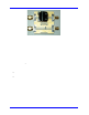
Table Of Contents
- Introduction TO QPHY-DDR3
- Signals measured
- DDR3 MEASUREMENT PREPARation
- Basic Functionality
- Using Qualiphy DDR3
- QualiPHY Compliance Test Platform
- QPHY-DDR3 Test Configurations
- 1) Clock tests DDR3-1333 (1 Probe)
- 2) CKdiff-DQse-DQSdiff 1333 Write Burst (3 Probes)
- 3) CKdiff-DQse-DQSdiff 1333 Read Burst (3 Probes)
- 4) Eye Diagram (3 Probes Debug)
- 5) Eye Diagram with CS Enabled (4 Probes Debug)
- 6) CKDiff-DQse-DQS-ADD/CTRLse (4 Probes Debug)
- 7) CKdiff-DQse-DQSp-DQsn (4 probes test, each DQS signal probed single ended)
- 8) CKp-CKn-DQse-DQSdiff (4 probe test, each CK signal is probed single ended)
- 9) Vref tests
- D1) Demo of All Tests
- QPHY-DDR3 Variables
- QPHY-DDR3 Limit Sets
- QPHY-DDR3 Tests
- Clock Tests
- tCK(avg), Average Clock Period
- tCK(abs), Absolute Clock Period
- tCH(avg), Average High Pulse Width
- tCL(avg), Average Low Pulse Width
- tCH(abs), Absolute High Pulse Width
- tCL(abs), Absolute Low Pulse Width
- tJIT(duty), Half Period Jitter
- tJIT(per), Clock Period Jitter
- tJIT(cc), Cycle to Cycle Period Jitter
- tERR(n per), Cumulative Error
- Eye Diagram
- Electrical Tests
- Timing Tests
- Four Probe tests measurements using ADDR/CTL
- Clock Tests

QPHY-DDR3 Software Opti on
917717 Rev C 7
INTRODUCTION TO QPHY-DDR3
QPHY-DDR3 is an automated test package performing all of the real time oscilloscope tests for Double
Data Rate in accordance with JEDEC Standard No. JESD79-3D.
The software can be run on the LeCroy SDA/DDA/WavePro 740Zi and 760Zi and all
SDA/DDA/WaveMaster 8Zi oscilloscopes.
Required equipment
• SDA/DDA/WavePro 740/760Zi or SDA/DDA/WaveMaster 8Zi oscilloscope.
• Four D620 Probes with WL-PLink ProLink probe body.
• Alternatively, D610 probes may be used if the voltage swing of the signal is within +/- 2.5Vp-p.
• TF-DSQ Probe Deskew and Calibration Fixture (not needed if using a Zi model oscilloscope).
SIGNA LS MEASURED
The compliance test requires probing the following signals (# refers to the negative polarity of the
differential signal):
CK, CK# I np ut
Clock: CK and CK# are differential clock inputs. All address and control input signals are sampled on the
crossing of the positive edge of CK and negative edge of CK#. Output (read) data is referenced to the
crossings of CK and CK# (both directions of crossing).
DQ Input/Output
Data Input/Output: Bi-directional data bus.
DQS, DQS# Input/Output
Data Strobe: outp ut w ith re ad data, input w ith write data. This signal is in phase with read data. The data
strobes DQS is paired with complementary signal DQS# to provide differential pair signaling to the system
during both reads and writes.
CS# Input
Chip Select: used onl y in m ulti-ranked systems. This is where 2 DIMM modules would be communicated
to on the same DDR3 bus. This signal is used to differentiate between the signals that were meant for
the DIMM the customer is measuring versus the signals that were meant for the other DIMM in the
system. Depending on the read and write latency of the system, the chip select signal is present on the
bus several clock cycles earlier than the actual read or write burst that is corresponds to. Be sure to set
the Overall Read Latency and Overall Write Latency variables when using the chip select signal.