
User Manual


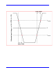

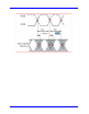
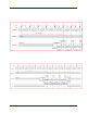

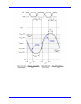
Table Of Contents
- Introduction TO QPHY-DDR3
- Signals measured
- DDR3 MEASUREMENT PREPARation
- Basic Functionality
- Using Qualiphy DDR3
- QualiPHY Compliance Test Platform
- QPHY-DDR3 Test Configurations
- 1) Clock tests DDR3-1333 (1 Probe)
- 2) CKdiff-DQse-DQSdiff 1333 Write Burst (3 Probes)
- 3) CKdiff-DQse-DQSdiff 1333 Read Burst (3 Probes)
- 4) Eye Diagram (3 Probes Debug)
- 5) Eye Diagram with CS Enabled (4 Probes Debug)
- 6) CKDiff-DQse-DQS-ADD/CTRLse (4 Probes Debug)
- 7) CKdiff-DQse-DQSp-DQsn (4 probes test, each DQS signal probed single ended)
- 8) CKp-CKn-DQse-DQSdiff (4 probe test, each CK signal is probed single ended)
- 9) Vref tests
- D1) Demo of All Tests
- QPHY-DDR3 Variables
- QPHY-DDR3 Limit Sets
- QPHY-DDR3 Tests
- Clock Tests
- tCK(avg), Average Clock Period
- tCK(abs), Absolute Clock Period
- tCH(avg), Average High Pulse Width
- tCL(avg), Average Low Pulse Width
- tCH(abs), Absolute High Pulse Width
- tCL(abs), Absolute Low Pulse Width
- tJIT(duty), Half Period Jitter
- tJIT(per), Clock Period Jitter
- tJIT(cc), Cycle to Cycle Period Jitter
- tERR(n per), Cumulative Error
- Eye Diagram
- Electrical Tests
- Timing Tests
- Four Probe tests measurements using ADDR/CTL
- Clock Tests
44 917717 Rev C
VIX(ac), AC Differential Input Cross Point Voltage
The typical value of VIX(ac) is expected to be about 0.5 x VDDQ of the transmitting device and VIX(ac) is
expected to track variations in VDDQ. VIX(ac) indicates the voltage at which differential input signals must
cross.
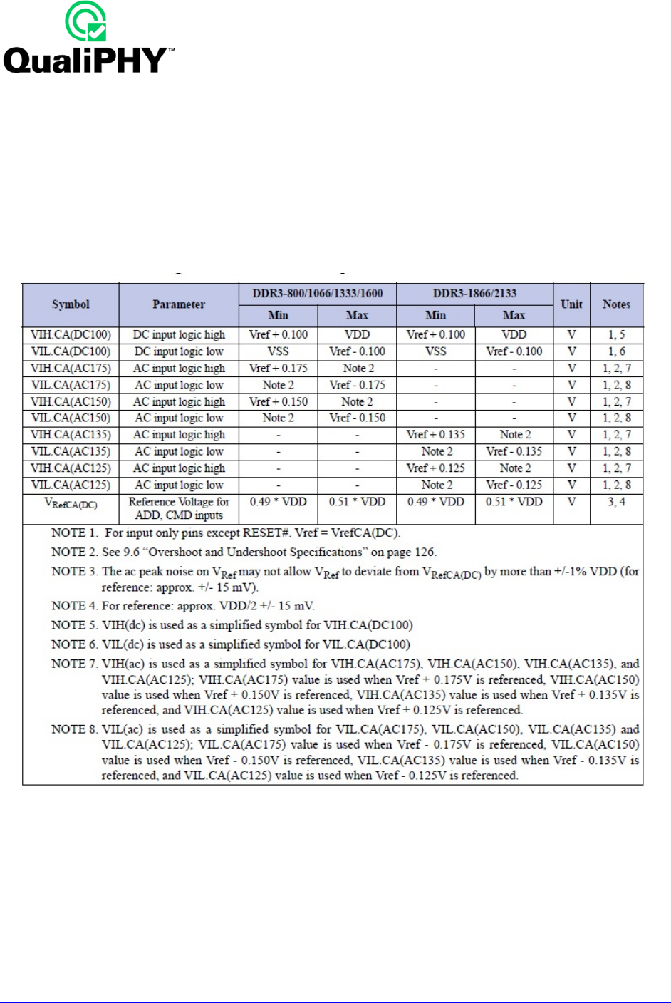
Vref(DC)
It is the linear average of Vref (t) over a very long period of time (e.g., 1 sec). This average has to meet
the min/max requirements in Table below. Furthermore V(t) may temporarily deviate from Vref(DC) by no
more than +/- 1% VDD.
Figure 22: Vref table (Table 23 from JESD79-3E)
§ § §