
User Manual


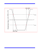

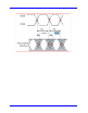
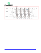

Table Of Contents
- Introduction TO QPHY-DDR3
- Signals measured
- DDR3 MEASUREMENT PREPARation
- Basic Functionality
- Using Qualiphy DDR3
- QualiPHY Compliance Test Platform
- QPHY-DDR3 Test Configurations
- 1) Clock tests DDR3-1333 (1 Probe)
- 2) CKdiff-DQse-DQSdiff 1333 Write Burst (3 Probes)
- 3) CKdiff-DQse-DQSdiff 1333 Read Burst (3 Probes)
- 4) Eye Diagram (3 Probes Debug)
- 5) Eye Diagram with CS Enabled (4 Probes Debug)
- 6) CKDiff-DQse-DQS-ADD/CTRLse (4 Probes Debug)
- 7) CKdiff-DQse-DQSp-DQsn (4 probes test, each DQS signal probed single ended)
- 8) CKp-CKn-DQse-DQSdiff (4 probe test, each CK signal is probed single ended)
- 9) Vref tests
- D1) Demo of All Tests
- QPHY-DDR3 Variables
- QPHY-DDR3 Limit Sets
- QPHY-DDR3 Tests
- Clock Tests
- tCK(avg), Average Clock Period
- tCK(abs), Absolute Clock Period
- tCH(avg), Average High Pulse Width
- tCL(avg), Average Low Pulse Width
- tCH(abs), Absolute High Pulse Width
- tCL(abs), Absolute Low Pulse Width
- tJIT(duty), Half Period Jitter
- tJIT(per), Clock Period Jitter
- tJIT(cc), Cycle to Cycle Period Jitter
- tERR(n per), Cumulative Error
- Eye Diagram
- Electrical Tests
- Timing Tests
- Four Probe tests measurements using ADDR/CTL
- Clock Tests
QPHY-DDR3 Software Opti on
917717 Rev C 41
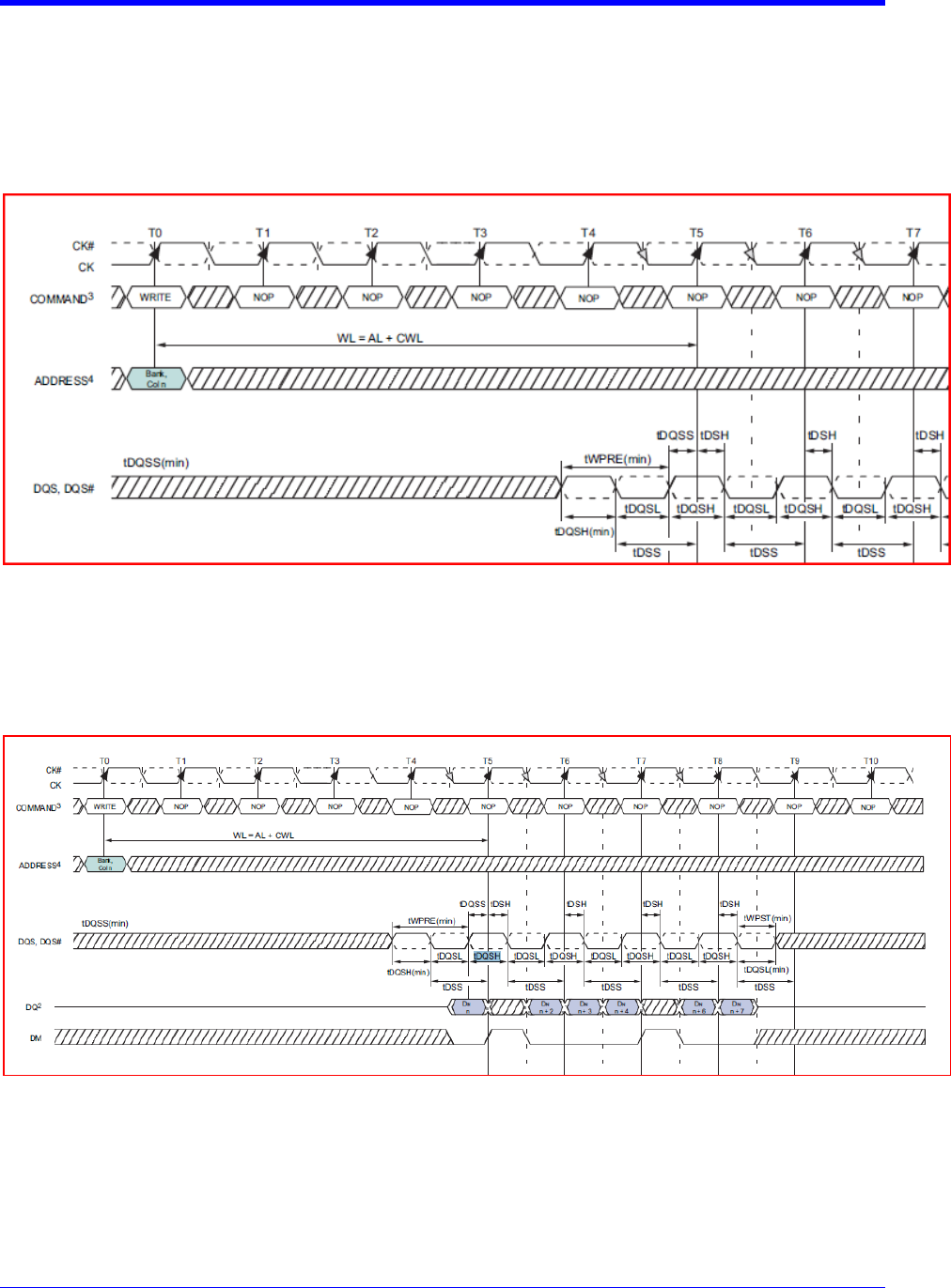
Write Bursts
tDQSS, DQS latching rising transitions to associated CK edge
CK rising edge at VREF level to DQS rising edge at VREF level, see Figure 21.
Figure 19. Burst write operation [JESD79-3D figure 43]
tDQSH, DQS Input High Pulse Width
DQS High pulse width at VREF level, see Figure 22.
Figure 20. Dat a input (write) timing [JESD79-3D figure 43]
tDQSL, DQS Input Low Pulse Width
DQS Low pulse width at VREF level, see Figure 22.