
User Manual


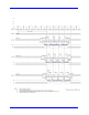


Table Of Contents
- Introduction TO QPHY-DDR3
- Signals measured
- DDR3 MEASUREMENT PREPARation
- Basic Functionality
- Using Qualiphy DDR3
- QualiPHY Compliance Test Platform
- QPHY-DDR3 Test Configurations
- 1) Clock tests DDR3-1333 (1 Probe)
- 2) CKdiff-DQse-DQSdiff 1333 Write Burst (3 Probes)
- 3) CKdiff-DQse-DQSdiff 1333 Read Burst (3 Probes)
- 4) Eye Diagram (3 Probes Debug)
- 5) Eye Diagram with CS Enabled (4 Probes Debug)
- 6) CKDiff-DQse-DQS-ADD/CTRLse (4 Probes Debug)
- 7) CKdiff-DQse-DQSp-DQsn (4 probes test, each DQS signal probed single ended)
- 8) CKp-CKn-DQse-DQSdiff (4 probe test, each CK signal is probed single ended)
- 9) Vref tests
- D1) Demo of All Tests
- QPHY-DDR3 Variables
- QPHY-DDR3 Limit Sets
- QPHY-DDR3 Tests
- Clock Tests
- tCK(avg), Average Clock Period
- tCK(abs), Absolute Clock Period
- tCH(avg), Average High Pulse Width
- tCL(avg), Average Low Pulse Width
- tCH(abs), Absolute High Pulse Width
- tCL(abs), Absolute Low Pulse Width
- tJIT(duty), Half Period Jitter
- tJIT(per), Clock Period Jitter
- tJIT(cc), Cycle to Cycle Period Jitter
- tERR(n per), Cumulative Error
- Eye Diagram
- Electrical Tests
- Timing Tests
- Four Probe tests measurements using ADDR/CTL
- Clock Tests
QPHY-DDR3 Software Opti on
917717 Rev C 15
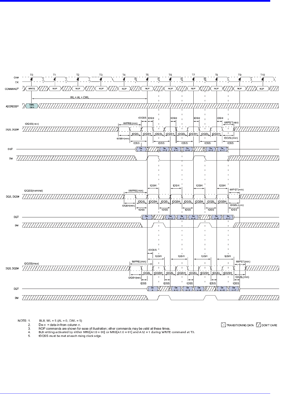
WRITE Burst Operation
During a READ or WRITE command, DDR3 supports BC4 and BL8 on the fly using address A12 during
the READ or WRITE (AUTO PRECHARGE can be enabled or disabled).
• A12 = 0, BC4 (BC4 = burst chop, tCCD = 4).
• A12 = 1, BL8.
• A12 is used only for burst length control, not as a column address.
Figure 7. Write Timing Definition a n d Parameters [JESD79-3D Figure 43]