QPHY-DDR3 DDR3 Serial Data Operator’s Manual 917717 Revision C – July 2011 Relating to the Following Release Versions: • Software Option Rev. 6.1 • DDR3 Script Rev. 1.1 • Style Sheet Rev. 1.
LeCroy Corporation 700 Chestnut Ridge Road Chestnut Ridge, NY, 10977-6499 Tel: (845) 578-6020, Fax: (845) 578 5985 Internet: www.lecroy.com © 2009 by LeCroy Corporation. All rights reserved. LeCroy and other product or brand names are trademarks or requested trademarks of their respective holders. Information in this publication supersedes all earlier versions. Specifications are subject to change without notice.
QPHY-DDR3 Software Option TABLE OF CONTENTS INTRODUCTION TO QPHY-DDR3 ............................................................................................ 7 Required equipment ................................................................................................................................................... 7 SIGNALS MEASURED .............................................................................................................. 7 CK, CK# Input ................................
Chip Select Signal Name .................................................................................................................................. 30 Script Settings .......................................................................................................................................................... 30 Save Acquired Waveforms ............................................................................................................................... 30 Silent mode control .....
QPHY-DDR3 Software Option VIH(dc), minimum DC input logic high ....................................................................................................................... 37 VIL(ac), maximum AC input logic low......................................................................................................................... 38 VIL(dc), minimum DC input logic low .........................................................................................................................
FIGURES Figure 1. READ Burst Operation RL = 5 (AL = 0, CL = 5, BL8) [JESD79-3D Figure 25]...................... 14 Figure 2. READ Burst Operation RL = 9 (AL = 4, CL = 5, BL8) [JESD79-3D Figure 26]...................... 14 Figure 3. Write Timing Definition and Parameters [JESD79-3D Figure 43] ......................................... 15 Figure 4. Report menu in QualiPHY General Setup ............................................................................... 17 Figure 5.
QPHY-DDR3 Software Option INTRODUCTION TO QPHY-DDR3 QPHY-DDR3 is an automated test package performing all of the real time oscilloscope tests for Double Data Rate in accordance with JEDEC Standard No. JESD79-3D. The software can be run on the LeCroy SDA/DDA/WavePro 740Zi and 760Zi and all SDA/DDA/WaveMaster 8Zi oscilloscopes. Required equipment • • • • SDA/DDA/WavePro 740/760Zi or SDA/DDA/WaveMaster 8Zi oscilloscope. Four D620 Probes with WL-PLink ProLink probe body.
DDR3 MEASUREMENT PREPARATION Before starting any test or data acquisition, the oscilloscope must be warmed for at least 20 minutes. Calibration is automatic under software control and no manual calibration is required. The procedure should be run again if the temperature of the oscilloscope changes by more than a few degrees. Deskewing the Probes Deskewing the probes is a mandatory requirement for running QPHY.
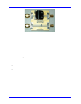
QPHY-DDR3 Software Option Figure 1. PCF200 Deskew Fixture A SMA male to BNC male 50-ohm cable is required to perform the calibration. System assembly is accomplished in the following steps: 1. Connect the BNC end of the 50 ohm cable to the oscilloscope AUX IN input. 2. Connect the SMA end of the 50 ohm cable to the SMA female connector on the PCF200 fixture. On oscilloscope models with a dedicated Fast Edge SMA output, 3a. Connect the PCF200 SMA male connector to the oscilloscope Fast Edge SMA output.
Figure 2.
QPHY-DDR3 Software Option The probe calibration menu can be accessed from the Vertical drop-down menu or from the channel dialog: Figure 3. Accessing the probe calibration menu Figure 4. Basic Probes Calibration menu The information in the probe calibration menu is organized such that each row represents the information for a given channel, and each column represents the calibration information or control for that channel.
1. Connect the probe to the PCF200 Fixture. 2. Press the Deskew Only button in the appropriate row representing the channel to be deskewed. Now you are ready to probe the circuit and perform your measurements. If power is interrupted during your measurements, reboot the oscilloscope and manually recall your settings.
QPHY-DDR3 Software Option BASIC FUNCTIONALITY The functionality is extracted from JEDEC Standard No. JESD79-3D, section 3. The DDR3 SDRAM is a high-speed dynamic random-access memory internally configured as an eightbank DRAM. The DDR3 SDRAM uses an 8n prefetch architecture to achieve high-speed operation. The 8n prefetch architecture is combined with an interface designed to transfer two data words per clock cycle at the I/O pins.
READ Burst Operation During a READ or WRITE command, DDR3 supports BC4 and BL8 on the fly using address A12 during the READ or WRITE (AUTO PRECHARGE can be enabled or disabled). • A12 = 0, BC4 (BC4 = burst chop, tCCD = 4). • A12 = 1, BL8. • A12 is used only for burst length control, not as a column address. Figure 5. READ Burst Operation RL = 5 (AL = 0, CL = 5, BL8) [JESD79-3D Figure 25] Figure 6.
QPHY-DDR3 Software Option WRITE Burst Operation During a READ or WRITE command, DDR3 supports BC4 and BL8 on the fly using address A12 during the READ or WRITE (AUTO PRECHARGE can be enabled or disabled). • A12 = 0, BC4 (BC4 = burst chop, tCCD = 4). • A12 = 1, BL8. • A12 is used only for burst length control, not as a column address. Figure 7.
USING QUALIPHY DDR3 QualiPHY DDR3 guides the user, step-by-step, through each of the source tests described in JEDEC Standard No. 79-3D. To do this, the user must setup a test session. Users choose test configurations to run.
QPHY-DDR3 Software Option Figure 8.
See the QualiPHY Operator’s Manual for more information on how to use the QualiPHY framework. Figure 9.
QPHY-DDR3 Software Option Oscilloscope Option Key Installation An option key must be purchased to enable the QPHY-DDR3 option. Call LeCroy Customer Support to place an order and receive the code. Enter the key and enable the purchased option as follows: 1. From the oscilloscope menu select Utilities Utilities Setup. 2. Select the Options tab and click the Add Key button. 3. Enter the Key Code using the on-screen keyboard. 4. Restart the oscilloscope to activate the option after installation.
QualiPHY tests the oscilloscope connection after clicking the Start button. The system prompts you if there is a connection problem. QualiPHY’s Scope Selector function can also be used to verify the connection. Please refer to the QualiPHY Operator’s Manual for explanations on how to use Scope Selector and other QualiPHY functions. Accessing the QPHY-DDR3 Software using QualiPHY This topic provides a basic overview of QualiPHY’s capabilities.
QPHY-DDR3 Software Option Figure 10.
4. Click the Configuration button in the QualiPHY main menu: 5. Select a configuration from the pop-up menu: Figure 11. QualiPHY configuration selection menu 6. Click Start. 7. Follow the pop-up window prompts.
QPHY-DDR3 Software Option Customizing QualiPHY The predefined configurations in the Configuration screen cannot be modified. However, you can create your own test configurations by copying one of the standard test configurations and making modifications. A description of the test is also shown in the description field when selected. Figure 12.
Once a custom configuration is defined, script variables and the test limits can be changed by using the Variable Setup and Limits Manager from the Edit/View Configuration window. Figure 13.
QPHY-DDR3 Software Option QPHY-DDR3 Operation After pressing Start in the QualiPHY menu, the software instructs how to set up the test using pop-up connection diagrams and dialog boxes. Figure 14. Start button Figure 15.
QPHY-DDR3 TEST CONFIGURATIONS Configurations include variable settings and limit sets as well, not just test selections. See the section for a description of each variable value and its default value. See the QPHY-DDR3 Limit Sets section for more information about the limit sets. 1) Clock tests DDR3-1333 (1 Probe) This configuration runs all of the clock tests. All of the variables are set to their defaults. The limit set in use is DDR3-1333.
QPHY-DDR3 Software Option • VOL(ac/dc) • VSWING • tQSH • tQSL • tHP, tQHS • tLZ(DQ) • tLZ(DQS) • tRPRE • tDQSS • tDQSH • tDQSL • tDIPW • tDSS • tDSH • tDS(base + derated) • tDH(base + derated) 917717 Rev C 27
3) CKdiff-DQse-DQSdiff 1333 Read Burst (3 Probes) This configuration runs all of the tests that are run on read bursts of the DDR3 signals in which 3 probes are required. All of the variables are set to their defaults. The limit set in use is DDR3-1333. The tests run are: • Eye Diagram – Read Bursts (Outputs) • SRQr • SRQf • tDQSQ • tQH • tDQSCK 4) Eye Diagram (3 Probes Debug) This configuration runs the Eye Diagram tests on both the read bursts and the write bursts.
QPHY-DDR3 Software Option • tIH (base + derated) • tIPW 7) CKdiff-DQse-DQSp-DQsn (4 probes test, each DQS signal probed single ended) • VSEH(ac) • VSEL(ac) • VIX(ac) • AC Overshoot Peak Amplitude • AC Overshoot Area above VDDQ • AC Undershoot Peak Amplitude • AC Undershoot Area below VSSQ • SlewR • SlewF 8) CKp-CKn-DQse-DQSdiff (4 probe test, each CK signal is probed single ended) • VSEH(ac) • VSEL(ac) • AC Overshoot Peak Amplitude • AC Overshoot Area above VDDQ • AC Undershoo
DQ Signal Name Select name of data (DQ) SUT. Choose between available DDR signal names. Default is DQ0. DQS Signal Name Select name of strobe (DQS) SUT. Choose between available DDR signal names. Default is DQS0. Clock Signal Name Select name of clock (CK) SUT. Choose between available DDR signal names. Default is CK. DUT Power Supply VDDQ Value of VDDQ used to compute test limits as specified by Jedec standard. Default is 1.5 V.
QPHY-DDR3 Software Option Overall Write Latency This is used to specify the Delay between DDR command (Write) to first data bit of related read burst. This is needed when using the Chip Select line to correctly identify read and write bursts in multi-ranked systems. This latency is measured in clock periods. Demo Settings Use Stored Waveforms When enabled, previously stored DDR3 waveforms is used. The default is No.
Advanced Settings Clock Period per Screen Division Oscilloscope timebase and sampling rate is set to acquire the given number of clock cycle per display horizontal division at a given DUT Speed Grad in MT/s and for a Max. Number of Samples Per Clock Period. The default is 3341 clock periods (this gives a 10us/div timebase at 667 MT/s and 3.3MS max for 100 samples per period). Timebase = [Clock Period Per Screen Division] / ([DUT Speed Grade in MT/s] / 2 * 1e6) Maximum Samples = [Max.
QPHY-DDR3 Software Option CAS Write Latency Allows the user to specify the CAS Write Latency (CWL) used to define tCK(avg) limits (see tables 61 to 64 in JEDEC Standard). Speed Bin Allows the user to specify the Speed Bin used to define tCK(avg) limits (see tables 61 to 64 in JEDEC Standard).
QPHY-DDR3 LIMIT SETS DDR3-800 This corresponds to the JEDEC JESD79-3D DDR3 standard specification limits for 800 MT/s. DDR3-1066 This corresponds to the JEDEC JESD79-3D DDR3 standard specification limits for 1066 MT/s. DDR3-1333 This corresponds to the JEDEC JESD79-3D DDR3 standard specification limits for 1333 MT/s.. DDR3-1600 This corresponds to the JEDEC JESD79-3D DDR3 standard specification limits for 1600 MT/s. QPHY-DDR3 TESTS Clock Tests All time measure on clock CK are done at level VREF.
QPHY-DDR3 Software Option tCL(avg), Average Low Pulse Width tCL(avg) is defined as the average low pulse width, as calculated across any consecutive 200 low pulses. tCH(abs), Absolute High Pulse Width tCH(abs) is the absolute instantaneous clock high pulse width, as measured from one rising edge to the following falling edge. tCL(abs), Absolute Low Pulse Width tCL(abs) is the absolute instantaneous clock low pulse width, as measured from one falling edge to the following rising edge.
tERR(n per), Cumulative Error tERR is defined as the cumulative error across n multiple consecutive cycles from tCK(avg). tERR is not subject to production test. There are 12 different tests: tERR(2per), tERR (3per), tERR (4per), tERR (5per), tERR(6per), tERR (7per), tERR (8per), tERR (9per), tERR (10per), tERR (11per), tERR (12per), tERR (13-50per), Eye Diagram Write Burst (Inputs) This is an informational only test that creates the eye diagram of all of the write bursts found in the acquisition.
QPHY-DDR3 Software Option For differential signals (e.g. CK - CK#) slew rate for rising edges is measured from Vihdiffmin to Vihdiffmax. This test is informational only. Figure 16. AC input test signal waveform [JESD79-3D figure 94] Logic Levels VIH(ac), maximum AC input logic high Measure the local maximum value from VREF to VREF of the high pulse histogram. If multiple pulses are measured, take the lowest number and the highest number as the worst cases.
The local minimum must be greater than or equal to the minimum limit. The local maximum must be less than or equal to the maximum limit. VIL(ac), maximum AC input logic low Measure the local minimum value from VREF to VREF of the low pulse histogram. If multiple pulses are measured, take the lowest number and the highest number as the worst cases. The lowest number must be greater than or equal to the minimum limit and the highest number must be less than or equal to the maximum limit.
QPHY-DDR3 Software Option Measure timing from DQS at VREF to DQ rising at VIH(ac)min and falling at VIL(ac)max. Figure 17 - Data output (read) timing [JESD79-3D figure 27] tQH, DQ/DQS Output Hold Time From DQS This measures the timing from DQS at VREF to DQ at VIH(dc) (rising edge) or VIL(dc) (falling edge). See figure 22. tDQSCK, DQS Output Access Time from CK/CK # Time from CK rising at VREF level to DQS rising at VREF level.
Figure 18. Burst read operation [JESD79-3D figure 28] This is a measure similar to tDQSS but on the Read frame (the result can be negative).
QPHY-DDR3 Software Option Write Bursts tDQSS, DQS latching rising transitions to associated CK edge CK rising edge at VREF level to DQS rising edge at VREF level, see Figure 21. Figure 19. Burst write operation [JESD79-3D figure 43] tDQSH, DQS Input High Pulse Width DQS High pulse width at VREF level, see Figure 22. Figure 20. Data input (write) timing [JESD79-3D figure 43] tDQSL, DQS Input Low Pulse Width DQS Low pulse width at VREF level, see Figure 22.
tDSS, DQS Falling Edge to CK Setup Time Time from DQS falling edge at VREF level to CK rising edge at VREF level, see Figure 22. tDSH, DQS Falling Edge Hold Time from CK Time from CK rising edge at VREF level to DQS falling edge at VREF level, see Figure 22.
QPHY-DDR3 Software Option Figure 21: tIS illustration (Figure 111 from JESD79-3E) Setup (tIS) nominal slew rate for a rising signal is defined as the slew rate between the last crossing of VREF(dc) and the first crossing of VIH(ac)min. Setup (tIS) nominal slew rate for a falling signal is defined as the slew rate between the last crossing of VREF(dc) and the first crossing of VIL(ac)max.
VIX(ac), AC Differential Input Cross Point Voltage The typical value of VIX(ac) is expected to be about 0.5 x VDDQ of the transmitting device and VIX(ac) is expected to track variations in VDDQ. VIX(ac) indicates the voltage at which differential input signals must cross. Vref(DC) It is the linear average of Vref (t) over a very long period of time (e.g., 1 sec). This average has to meet the min/max requirements in Table below.