
User's Manual


VI-3
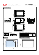
RESET – Tactile switch resets the monitor and control system. The amplifier gets shut down for
under 0.5 seconds and comes back on with each depress of the reset button. At the same time,
all fault counters in the microcontroller software are reset and the LCD is reset in the same
manner as it is with a depress of the NAVIGATE button. Reset switches are individual to each
enclosure but may be tied together externally through the remote port, as explained later in this
section.
The buzzer control comes from pin 7 on microcontroller U114. The control signal turns on the base
of transistor Q101, which allows current to flow through the single tone magnetic buzzer. Jumper
J105 simply turns off the buzzer.
The carrier disable circuit simply applies a shutdown voltage to the driver pallet in the system. The
U114 generates the signal out of pin 21 and controls transistor Q102 through R117. When Q102 is
turned off, the shutdown voltage to the driver is floating and the carrier is on. During a fault
condition, when Q102 is turned on, the shutdown voltage is applied to the carrier disable on the
driver. Relay K101, which outputs the carrier disable, is protected from transient spikes by D104.
Signal Conditioning Components
The signal processing section of the Series II – rev I PCBs is used to buffer potentially noisy or
damaging signals from the ADC. Power supply samples and forward and reflected power from a
directional coupler are then digitized.
Firstly, all analog signals are protected with a resettable fuse and transient voltage suppressor
(TVS) combination. These components ensure that voltages above the Vbr breakdown voltage of
the TVS get clamped and do not pass farther down the circuit. After this protection stage, the
analog voltages get dropped with voltage dividers to safe levels for the buffers and ADC. For
example, a 30Vdc power supply sample gets dropped to a level below the +2.5Vdc voltage
reference of the ADC. After the voltage dividers, the analog signals get buffered with U107 and
U108, configured as unity gain voltage followers. Finally, after some further decoupling capacitors
and filters, the analog signals get digitized by the 8-channel, 10-bit ADC (U10) and sent to the
microcontroller through a serial interface.
In the power amplifier and filter enclosures, there are (3) analog voltages that get conditioned and
processed: DC power supply sample, forward RF power, and reflected RF power. Specifically, the
components for the power amplifier and filter enclosure conditioning are as follows:
DC power supply – J108 (pin 1 floating and direct connection), F107, C120, L108,
C121, R129, R130, VR105, U8, C122, C123, L109, C124 and
U10.
Forward RF power – J108 (pin 2), F106, D109, C117, C118, L107, C119, R127, VR104,
R128, U108, C108, C125, L110, C126, C127, and U110.
Reflected RF power – J108 (pin 3), F105, D108, C114, C115, L106, C116, R125, VR103,
R126, U108, C130, L112, C131, C132, and U110.