
User Manual

VI-4
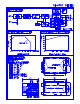
Signal Conditioning Components
The signal processing section of the Series II-H PCBs is used to buffer potentially noisy or
damaging signals from the ADC. Power supply samples and forward and reflected power from a
directional coupler are then digitized.
Firstly, all analog signals are protected with a resettable fuse and transient voltage suppressor
(TVS) combination. These components ensure that voltages above the Vbr breakdown voltage of
the TVS get clamped and do not pass farther down the circuit. After this protection stage, the
analog voltages get dropped with voltage dividers to safe levels for the buffers and ADC. For
example, a 28Vdc power supply sample gets dropped to a level below the +5Vdc supply voltage of
the ADC. After the voltage dividers, the analog signals get buffered with U7 and U8, configured as
unity gain voltage followers. Finally, after some further decoupling capacitors and filters, the analog
signals get digitized by the 8-channel, 10-bit ADC (U10) and sent to the microcontroller through a
serial interface.
In the power amplifier and filter enclosures, there are (3) analog voltages that get conditioned and
processed: DC power supply sample, forward RF power, and reflected RF power. Specifically, the
components for the power amplifier and filter enclosure conditioning are as follows:
DC power supply sample – J7 (pin8), F9, D11, R32, R33, U8, C33, C34, C35, and U10.
Forward RF power – J7 (pin7), F8, D10, R30, R31, U8, C29, C30, C31, and U10.
Reflected RF power – J7 (pin6), F7, D9, R28, R29, U8, C26, C27, C28, AND U10.
In the power supply enclosure, there are (2) power supplies, but they are both paralleled together.
Hence, only (1) analog voltage is conditioned and processed for the LCD. Specifically, the
components for the power supply sample are as follows:
DC power supply sample- J7 (pin8), F9, D11, R32, R33, U8, C33, C34, C35, and U10.