P-379 PROCESSOR 1 P-379 Processor
TABLE OF CONTENTS 1.0 SAFEGUARDS ...................................................................................................................3 General Safeguards ..............................................................................................................3 Safety and First Aid...............................................................................................................4 2.0 WARRANTY.....................................................................................
1.0 SAFEGUARDS General Safeguards This section is written as a general guide for those having previous knowledge and experience with these kinds of equipment. It is not intended to contain a complete statement of all safety precautions, which should be observed by personnel using this or other electronic equipment. To reduce the risk of fire or electric shock, do not expose this equipment to rain or moisture. Do not open the cabinet. Refer servicing to qualified personnel. 1.
Safety and First Aid Personnel engaged in the installation, operation, maintenance, or servicing of electronic equipment are exposed to the hazard of high voltage. It is imperative that all safety regulations and precautions are consistently observed. Knowledge of first aid procedures is recommended. The following information is presented as a reference only. DANGEROUS VOLTAGES AND CURRENTS MAY BE PRESENT IN THE EQUIPMENT EVEN THOUGH THE POWER IS OFF.
2.0 WARRANTY Technalogix Ltd. products have been completely tested and found to meet specifications and be in proper operating condition. They are warranted to be free from defects in materials and workmanship for a period of one year from the date of shipment. Technalogix Ltd. will not be liable for damages of whatever nature arising out of or in connection with the equipment or its use thereof.
3.0 DESCRIPTION AND SPECIFICATIONS General Description The P-379 contains the latest in television electronics, including synthesized crystalreferenced phase-locked-loop oscillators, microprocessor control, saw-filtered if and hybrid amplifiers. In addition to these features, the U.S. version contains automatic input offset programming to remove input offsets inherent to off-air channels (0, ±10KHz), cable standard channels (0, +12.5KHz, +25KHz) and Cable HRC channels (0.3KHz master oscillator offset).
HRC Output Frequency Set: This Technalogix frequency agile product can be set for HRC frequency output. This feature is controlled by an internal dip switch assembly, DS-1. The switch is located near the right front corner (with the panel facing you) between the test point and the output converter module. DS-1 is clearly marked on the PCB. Switch #3 placed in the OFF position switches the output frequency to HRC on all channels. The switch is normally set to ON at the factory.
NTSC Video Characteristics System M/N NTSC 75Ohms, unbalanced 7 to 800 MHz 54 to 890 MHz 6.0Mhz -16 to +16 dBmV Sync Tip Ref.
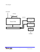
Block Diagram Pre-Amp IN RF Loop Pre-Amp Out RF In IF Carrier Up converter Tuner PCB Down converter Display and Control Board Output Amplifier RF Output 9 P-379 Processor
4.0 INSTALLATION This section contains installation recommendations, unpacking, inspection, and installation instructions for the Technalogix P-379 Processor. Carefully read all material in this section prior to installation. Also read and review operating procedures later in this section. Building Recommendations The quality of the building is of great importance if you are to expect long life and continued performance from the processor. The building must be clean, dry, temperature controlled and secure.
Electrical Service Recommendations Technalogix recommends that a qualified, licensed local electrician be consulted for the required electrical service. We suggest local electricians because: • The personnel knows the local codes • The personnel can be on site readily • You are apt to get better overall support if you give what business you can to local suppliers Technalogix recommends that proper AC line conditioning and surge suppression be provided on the primary AC input to the power amplifier.
Antenna and Tower Recommendations Your preliminary engineering workgroup should establish your antenna and tower requirements, both for receiving and transmitting antennas. Construction of sturdy, high quality antenna/tower systems will pay off in terms of coverage of your service area, the overall quality and saleability of your radiated signal, and reduced maintenance expenses. Technalogix provides complete turnkey antenna systems if needed.
Unpacking and Inspection Check the outside of the container. Carefully open the container and remove the processor. Retain all packing material that can be reassembled in the event that the equipment must be returned to the factory. Exercise care in handling equipment during inspection to prevent damage due to rough or careless handling. Visually inspect the enclosure of the processor for damage that may have occurred during shipment.
Location and Function of Controls and Connectors The following illustrations depict the location of the installation connectors when installing the power amplifier with a processor. FRONT BACK Aural Carrier Level - Allows user to set aural carrier level relative to visual carrier level. Processor is factory tested at –10 dBc (decibels below visual carrier). Input Source – Allows the user to select between cable HRC, cable standard or off-air.
RS-232 Ports – Set up for optional RS-232 control option. Combined IF Input/ Output – 45.75 MHz visual carrier and 41.25 MHz audio carrier intermediate frequency signal loop. RF In – Modulated RF input – Recommended RF input is 0 dBmV to 5 dBmV. T-Channel Switch – Allows the user to switch the optional T-channel on or off. To use the T-Channel Input Option, if the unit is so equipped, ensure that that a T-channel input source is attached to the F-connector marked “T-Channel IN” on the rear panel.
5.0 OPERATING PROCEDURE Preliminary Hook-up 1. Position the Technalogix P-379 agile processor in its installation mount or rack. 2. Locate the antenna lead or cable drop that will provide the input signal for the P379 agile processor. 3. Ensure that the input signal provides an adequate signal. The recommended input level for best performance from the Technalogix P-379 Processor is 0 to +10dBmV (+60dBuV to +70dBuV). Setup and Operation 1.
4. Input channel selection. Select the desired input source type and channel using the front panel controls. Because the built-in input offset feature automatically removes any input offset, no calculations or adjustments are required. The Technalogix P-379 Agile Processor has a built-in delay in the input- and outputchannel tuning circuits. In order to change channels, hold the channel select switch in the up- or down-position for at least three seconds.
5. Select the desired output channel. Unless otherwise specified, the unit is factory set for cable standard channel frequencies and the microprocessor automatically selects the proper FCC offset for the output channels, requiring no calculations or adjustments. NOTE: For HRC output channels, see the section in this manual entitled HRC Output Frequency Set. During output-channel tuning, the FREQUENCY LOCK LED on the front panel display may also blink during input-channel tuning.
8. While the RF OUTPUT signal is still connected to the spectrum analyzer or field strength meter, observe the aural carrier level. The difference between the video carrier level and the audio carrier level – the “Delta AV” or ΔAV – should be the same as the input source. In other words, if the RF INPUT signal ΔAV is 13dB, the RF OUTPUT signal ΔAV should be 13dB ±2dB.
Translator Hookup 1. Connect modulated video from P-379 RF OUT to the Technalogix power amplifier. 2. Turn down RF level on P-379 all the way. 3. Ensure that IF OUT is connected to IF IN on the P-379 processor using the loop F to F cable supplied. 4. Connect the transmitting antenna cable to the RF output connector on the power amplifier. It is recommended that a quality through line wattmeter be installed in this same line. 5. Verify that all signal and RF cables are connected properly. 6.
6.0 PROBLEM TROUBLESHOOTING GUIDE The guide below covers some typical symptoms, possible associated causes and suggested actions to follow before returning the unit for repair. It is not meant to be allinclusive.
7.0 BILL OF MATERIALS, SCHEMATICS, AND PCB OVERLAYS Agile Logic Board Bill of Materials Last Revision: 09.12.00 Component Reference Quantity Identification C1 C10 C11 C12 C13 C14 C15 C16 C17 C18 C19 C2 C20 C21 C22 C23 C24 C3 C4 C5 C6 C7 C8 C9 D1 D2 D3 DS1 JP1 JP2 JP3 JP4 JP5 JP6 JP7 JP8 L1 1 1 1 1 1 1 1 1 1 1 1 1 1 1 1 1 1 1 1 1 1 1 1 1 1 1 1 1 1 1 1 1 1 1 1 1 1 22pF 0.47uF 10 uF 22 uF 22 uF 22 uF 22 uF 0.01uF 0.01uF 47 uF 47 uF 22pF Modifier 0.01uF 0.01uF 0.01uF 0.01uF 22 uF 10 uF 0.47uF 0.47uF 0.
L2 L3 L4 L5 P1 P10 P11 P12 P2 P3 P4 P5 1 1 1 1 1 1 1 1 1 1 1 1 P6 P7 P8 P9 Q1 Q2 QP1 R1 R10 R11 R12 R13 R14 R15 R16 R17 R18 R19 R2 R20 R21 R22 R23 R3 R4 R5 R6 R7 R8 R9 RP1 RP2 1 1 1 1 1 1 1 1 1 1 1 1 1 1 1 1 1 1 1 1 1 1 1 1 1 1 1 1 1 1 1 1 6T 6T 6T 6T 4 PIN 10 POS 4 PIN 8 POS RT ANG F 12 POS 12 POS ON DISPLAY BDS 12 POS 12 POS 4 PIN 10 PIN 2222 2907 4-2222A 10 MΩhm 1 kΩhm 5 kΩhm 10 KΩhm 10 KΩhm 1 kΩhm 6.8 kΩhm 1 kΩhm 500 Ωhm 10 KΩhm 5.6 kΩhm 4.
RP3 RP4 RP5 SW1 SW2 SW3 SW4 U1 U2 U3 U4 U5 U6 U7 U8 Y1 1 1 1 1 1 1 1 1 1 1 1 1 1 1 1 1 10 kΩhm 150 Ωhm 150 Ωhm PADDLE PADDLE ROCKER ROCKER MC74HC165 IC34064 68705C8 74H04 74H04 MC14499 DS232 X2402 4MHz 24 DIPIL11 DIP IL8 DIP IL8 SW1 SW1 SW1 SW1 DIP16C REGTO92 DIP40C DIP14C DIP14C DIP18C DIP16C DIP8C XTAL P-379 Processor
1 2 3 4 5 6 7 8 9 10 5V 5V R11 +12V 1 IN RP3 U7 1 2 3 4 5 6 7 8 16 15 14 13 12 11 10 9 R18 MUTE Q1 D4 R16 360 VIDEO MODULATION C3 C12 + 1 2 3 4 5 6 7 8 1 2 37 36 34 22 21 C14 + 2 3 4 5 6 9 10 1 U11 P8 P7 P6 P5 RSTX RSRX RDI TDO R8 LD LDI C1 C10 R7 R6 LDO C6 C5 1 1 1 1 1 C9 EEPROM MEMORY STORAGE 32 U8 C P1 P2 P3 P4 RP5 5V P8 P7 P6 P5 1 2 3 4 5 6 7 8 C2 U9 18 17 16 15 14 13 12 11 10 RP4 1 2 3 4 5 6 7 8 9 JP2 1 2 3 4 5 6 7 8 9 10 11 12 13 14 15 16 17 18 19
Agile Output Amplifier Bill of Materials Last Revision: 09.12.00 Component Reference C1 C2 C3 C4 C5 C6 C7 E1 E2 E3 E5 I1 L1 L2 L3 L4 L5 P1 U1 Quantity Identification 1 1 1 1 1 1 1 1 1 1 1 1 1 1 1 1 1 1 1 0.1uF 0.1uF 2.7 pF 3-10pF 3-10pF 3-10pF 2.
1 2 3 4 5 6 7 A A B B E2 +24V L1 C C C1 C2 D D L2 1 L3 L4 L5 9 E 2 E 5 U1 + INPUT E1 C3 C4 C5 C6 C7 R1 P1 OUTPUT F F E3 -20dB TEST G G H H I I Technalogix Ltd.
Agile Up Converter Board Bill of Materials Last Revision: 09.13.
C136 C137 C138 C139 C14 C140 C141 C15 C16 C17 C18 C19 C2 C204 C205 C206 C207 C208 C209 C21 C210 C22 C3 C300 C301 C303 C4 C5 C6 C7 C8 C9 D1 D100 D101 D102 D103 D2 D3 F1 FT200 J1 J10 J2 J3 J4 J5 1 1 1 1 1 1 1 1 1 1 1 1 1 1 1 1 1 1 1 1 1 1 1 1 1 1 1 1 1 1 1 1 1 1 1 1 1 1 1 1 1 1 1 1 1 1 1 (VALUE) (VALUE) (VALUE) (VALUE) (VALUE) (VALUE) (VALUE) (VALUE) (VALUE) (VALUE) (VALUE) (VALUE) (VALUE) (VALUE) (VALUE) (VALUE) (VALUE) (VALUE) (VALUE) (VALUE) (VALUE) (VALUE) (VALUE) (VALUE) (VALUE) (VALUE) (VALUE) (VALUE)
J6 J7 J8 J9 L1 L100 L101 L102 L103 L104 L105 L106 L108 L109 L2 L3 L4 L5 L6 M1 OSC1 P1 P2 Q1 Q2 R1 R10 R101 R102 R103 R104 R105 R106 R107 R108 R109 R11 R111 R112 R113 R116 R117 1 1 1 1 1 1 1 1 1 1 1 1 1 1 1 1 1 1 1 1 1 1 1 1 1 1 1 1 1 1 1 1 1 1 1 1 1 1 1 1 1 1 (VALUE) (VALUE) (VALUE) (VALUE) (VALUE) (VALUE) (VALUE) (VALUE) (VALUE) (VALUE) (VALUE) (VALUE) (VALUE) (VALUE) (VALUE) (VALUE) (VALUE) (VALUE) (VALUE) THRU-HOLE THRU-HOLE THRU-HOLE THRU-HOLE 1812 1210 1210 1210 1210 1812 1210 1210 1210 1210 1812 18
R123 R13 R14 R15 R16 R17 R18 R19 R2 R20 R203 R204 R205 R206 R207 R21 R22 R23 R24 R25 R26 R3 R4 R5 R6 R7 R8 R9 U100 U101 U2 U200 1 1 1 1 1 1 1 1 1 1 1 1 1 1 1 1 1 1 1 1 1 1 1 1 1 1 1 1 1 1 1 1 (VALUE) (VALUE) (VALUE) (VALUE) (VALUE) (VALUE) (VALUE) (VALUE) (VALUE) (VALUE) (VALUE) (VALUE) (VALUE) (VALUE) (VALUE) (VALUE) (VALUE) (VALUE) (VALUE) (VALUE) (VALUE) (VALUE) (VALUE) (VALUE) (VALUE) (VALUE) (VALUE) (VALUE) 31 1206 1206 1206 1206 1206 1206 1206 1206 1206 1206 1206 RES2010A 1206 1206 1206 1206 1206
1 2 3 4 5 6 7 8 9 10 +12V J7 +12V +12V C13 + C9 C300 C301 A L4 C2 C1 1uF L5 C207 C209 A C206 C210 R12 R1900 C12 C7 L3 R11 R1800 R1 C1 D1 C229 C6 C10 R14 + L2 R22 L6 U1 R8 C11 R16 C15 + U2 R24 R13 C3 D2 D3 C3 R15 R7 L1 R23 FILL U4 R201 P1 C201 R25 FILL200 R17 C204 + U200 C205 R203 R200 C4 R204 R202 C208 R20 C14 +12V R4 R2 B R5 B C130 R6 U3 R21 R205 R207 IF MIXER R3 IF OUT P2 J10 R206 R123 R121 R122 LOCK DETECT TO MPU D10
750 MHz down Converter Board Bill of Materials Last revised: 09.13.
C136 C137 C138 C139 C14 C140 C141 C15 C16 C17 C18 C19 C2 C204 C205 C206 C207 C208 C209 C21 C210 C22 C3 C300 C301 C303 C4 C5 C6 C7 C8 C9 D1 D100 D101 D102 D103 D2 D3 F1 FT200 J1 J10 J2 J3 J4 J5 1 1 1 1 1 1 1 1 1 1 1 1 1 1 1 1 1 1 1 1 1 1 1 1 1 1 1 1 1 1 1 1 1 1 1 1 1 1 1 1 1 1 1 1 1 1 1 (VALUE) (VALUE) (VALUE) (VALUE) (VALUE) (VALUE) (VALUE) (VALUE) (VALUE) (VALUE) (VALUE) (VALUE) (VALUE) (VALUE) (VALUE) (VALUE) (VALUE) (VALUE) (VALUE) (VALUE) (VALUE) (VALUE) (VALUE) (VALUE) (VALUE) (VALUE) (VALUE) (VALUE)
J6 J7 J8 J9 L1 L100 L101 L102 L103 L104 L105 L106 L108 L109 L2 L3 L4 L5 L6 M1 OSC1 P1 P2 Q1 Q2 R1 R10 R101 R102 R103 R104 R105 R106 R107 R108 R109 R11 R111 R112 R113 R116 R117 R118 R119 R12 R121 R122 1 1 1 1 1 1 1 1 1 1 1 1 1 1 1 1 1 1 1 1 1 1 1 1 1 1 1 1 1 1 1 1 1 1 1 1 1 1 1 1 1 1 1 1 1 1 1 (VALUE) (VALUE) (VALUE) (VALUE) (VALUE) (VALUE) (VALUE) (VALUE) (VALUE) (VALUE) (VALUE) (VALUE) (VALUE) (VALUE) (VALUE) (VALUE) (VALUE) (VALUE) (VALUE) (VALUE) (VALUE) (VALUE) (VALUE) (VALUE) (VALUE) (VALUE) (VALUE)
R123 R13 R14 R15 R16 R17 R18 R19 R2 R20 R203 R204 R205 R206 R207 R21 R22 R23 R24 R25 R26 R3 R4 R5 R6 R7 R8 R9 U100 U101 U2 U200 1 1 1 1 1 1 1 1 1 1 1 1 1 1 1 1 1 1 1 1 1 1 1 1 1 1 1 1 1 1 1 1 (VALUE) (VALUE) (VALUE) (VALUE) (VALUE) (VALUE) (VALUE) (VALUE) (VALUE) (VALUE) (VALUE) (VALUE) (VALUE) (VALUE) (VALUE) (VALUE) (VALUE) (VALUE) (VALUE) (VALUE) (VALUE) (VALUE) (VALUE) (VALUE) (VALUE) (VALUE) (VALUE) (VALUE) 36 1206 1206 1206 1206 1206 1206 1206 1206 1206 1206 1206 RES2010A 1206 1206 1206 1206 1206
1 2 3 4 5 6 7 8 9 10 A A 12V C215 12V C48 U16 FILTER C100 C47 C212 C213 RF C101 R100 R102 R200 R104 R208 R212 P1 C43 R202 C42 U4 R205 L200 R204 L202 L201 L203 R207 C210 U201 C211 R209 R211 RF OUT R103 L100 C102 R101 LO C205 C200 R212 R203 R201 R206 C206 C207 C208 P3 C214 C209 R210 B B L204 R20 C39 R18 R19 C C LOCK DETECT TO MPU D1 C4 R2 12V R5 Y1 C3 C2 12V R8 R3 C1 4.
Power Supply Board Bill of Materials Last Revised: 09.12.00 Component Reference Quan tity C1 1 C10 1 C11 1 C12 1 C13 1 C14 1 C15 1 C16 1 C17 1 C18 1 C19 1 C2 1 C3 1 C4 1 C5 1 C6 1 C7 1 C8 1 C9 1 P1 1 P2 1 P3 1 P4 1 P5 1 P6 1 P7 1 R1 1 R2 1 R4 1 U1 1 U2 1 U3 U4 U5 U6 U7 Identification Modifier Package 4700 0.1 uF 0.1 uF 0.1 uF 0.1 uF 1000 0.1 uF 4700 1000 0.1 uF 0.1 uF 4700 0.1 uF 0.1 uF 0.1 uF 0.1 uF 2200 0.
2 3 U4 7824 1 IN A 4 U6 7805 +24V OUT 3 1 IN 7 +5V OUT 3 2 + + 6 A COM 2 COM C4 5 C1 C5 C7 + 1 C12 C15 U5 7812 1 IN B 3 C16 +12V OUT 3 B C2 4 + + 2 COM C8 C10 C9 1 U1 2 C11 C13 P1 C C 1 2 3 4 5 6 3 4 R1 P6 1 1 2 3 4 5 6 U2 2 D P5 1 2 3 4 5 6 P4 P3 1 2 3 4 5 6 1 2 3 4 5 6 P2 1 2 3 4 5 6 P7 1 2 3 4 5 6 7 8 +24V +30V GND +5V +12V GND D C19 C18 3 4 1 2 U7 E E OUT 3 + 2 COM C17 C3 +30V R2 + U3 LM317 1 IN C6 C14 F F R4 G G H
Tuner Processor Board Bill of Materials Last Revised: 09.13.00 Component Reference Quantity Identification C1 C100 C100 C101 C11 C13 C14 C15 C16 C17 C18 C19 C2 C20 C21 C22 C23 C24 C25 C26 C27 C28 C29 C3 C30 C36 C37 C38 C39 C4 C40 C41 C42 C43 C44 C45 C46 C47 C48 C49 C5 C50 1 1 1 1 1 1 1 1 1 1 1 1 1 1 1 1 1 1 1 1 1 1 1 1 1 1 1 1 1 1 1 1 1 1 1 1 1 1 1 1 1 1 0.47 uF 0.001 uF 0.01 uF 0.1 uF 0.47 uF 0.1 uF 0.1 uF 0.01 uF 0.01 uF 0.1 uF 0.1 uF 0.01 uF 0.47 uF 0.01 uF 0.1 uF 8.
C51 C52 C53 C54 C55 C56 C57 C58 C59 C6 C60 C61 C62 C63 C64 C65 C66 C67 C68 C69 C7 C70 C71 C72 C73 C74 C75 C76 C77 C78 C79 C8 C80 C81 C82 C83 C84 C85 C86 C87 C88 C89 C9 C90 C91 C92 C93 1 1 1 1 1 1 1 1 1 1 1 1 1 1 1 1 1 1 1 1 1 1 1 1 1 1 1 1 1 1 1 1 1 1 1 1 1 1 1 1 1 1 1 1 1 1 1 0.01 uF 47 uF 0.001 uF 0.47 uF 0.1 uF 22 pF 47 pF 0.01 uF 0.1 uF 0.01 uF 0.1 uF 4.7 pF 0.01 uF 0.1 uF 0.1 uF 100 pF 0.1 uF 0.1 uF 0.01 uF 68 pF 0.47 uF 33 pF 4.5-20 pF 0.01 uF 0.1 uF 100 pF 0.01 uF 0.01 uF 0.1 uF 0.01 uF 0.01 uF 0.
C94 C95 C96 C97 C98 C99 D2 D3 D4 D5 D6 E1 E2 F1 GND JP2 JP3 JP4 JP5 JP6 L1 L10 L11 L12 L13 L14 L15 L16 L17 L18 L2 L3 L5 L6 L7 L9 P1 P2 P3 P4 Q1 Q2 Q4 Q5 Q6 Q7 Ω 1 1 1 1 1 1 1 1 1 1 1 1 1 1 1 1 1 1 1 1 1 1 1 1 1 1 1 1 1 1 1 1 1 1 1 1 1 1 1 1 1 1 1 1 1 1 Ω 0.01 uF 0.01 uF 0.01 uF 0.1 uF 0.
R1 R12 R13 R14 R15 R16 R17 R18 R19 R2 R20 R21 R22 R23 R24 R25 R26 R27 R28 R29 R3 R30 R31 R32 R33 R34 R35 R36 R37 R38 R39 R4 R40 R41 R42 R43 R44 R45 R46 R47 R48 R49 R5 R50 1 1 1 1 1 1 1 1 1 1 1 1 1 1 1 1 1 1 1 1 1 1 1 1 1 1 1 1 1 1 1 1 1 1 1 1 1 1 1 1 1 1 1 1 4.7 Ωhm 1.5 kΩhm 18 Ωhm 680 Ωhm 680 Ωhm 3.9 kΩhm 2 kΩhm 430 Ωhm 100 kΩhm 0 Ωhm 10 kΩhm 10 kΩhm 12 kΩhm 7.5 kΩhm 4.7 Ωhm 4.7 kΩhm 1 kΩhm 10 kΩhm 10 MΩhm 3.3 kΩhm 0 Ωhm 10 MΩhm 100 Ωhm 10 kΩhm 10 kΩhm 4.7 Ωhm 560 Ωhm 220 Ωhm 56 Ωhm 220 Ωhm 4.
R51 R52 R53 R54 R55 R56 R57 R58 R59 R6 R60 R61 R62 R63 R64 R65 R66 R67 R68 R69 R7 R70 R71 R72 R73 R74 R75 R76 R77 R78 R79 R8 R80 R81 R82 R83 R84 R85 R86 R87 R88 R89 R90 R91 R92 R93 1 1 1 1 1 1 1 1 1 1 1 1 1 1 1 1 1 1 1 1 1 1 1 1 1 1 1 1 1 1 1 1 1 1 1 1 1 1 1 1 1 1 1 1 1 1 4.7 Ωhm 470 kΩhm 470 kΩhm 680 kΩhm 4.7 kΩhm 4.7 Ωhm 470 kΩhm 470 kΩhm 680 kΩhm 39 Ωhm 39 kΩhm 100 kΩhm 4.7 Ohm 680 Ohm 560 kOhm 5.6 kOhm 100 kOhm 4.7 Ohm 1 kOhm 2 kOhm 51 Ohm 12 Ohm 82 Ohm 220 Ohm 75 Ohm 1 kOhm 1 kOhm 2 kOhm 4.
R94 R95 R96 R97 R98 R99 SW1 TP1 TP2 TP3 TP4 TUNER U1 U2 U3 U4 U5 Y1 Y2 1 1 1 1 1 1 1 1 1 1 1 1 1 1 1 1 1 1 1 6.
1 2 3 4 5 6 7 8 9 10 +12 C7 +12 R2 +29.7V R73 C14 U1 C91 C8 R69 BT R3 A L15 .47 +29.7V +5V L16 .47 + C15 AGC C19 R72 C9 TP1 R80 C13 L17 .47 R76 +5V AGC TEST POINT C20 A R79 CLOCK U2 +9V R6 C17 R8 DATA 5 R7 ENABLE R83 C24 1 C21 Q1 GND Clock C18 MFV-2 R81 C22 R82 C26 R75 R74 R70 Q2 GND GND R4 GND GND IF C16 R5 D3 +12V D2 R77 C11 D1 C12 2.5-20pF L4 .47 C2 C92 R71 C30 R12 Data C23 L5 .47 L6 .47 C27 C28 C29 C25 L8 .
Thank you for choosing Technalogix Ltd.