
Integration Manual
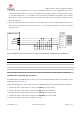


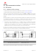
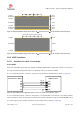
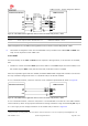

Table Of Contents
- Contents
- 1 System description
- 1.1 Overview
- 1.2 Architecture
- 1.3 Pin-out
- 1.4 Operating modes
- 1.5 Supply interfaces
- 1.5.1 Module supply input (VCC)
- 1.5.1.1 VCC supply requirements
- 1.5.1.2 VCC current consumption in 2G connected mode
- 1.5.1.3 VCC current consumption in 3G connected mode
- 1.5.1.4 VCC current consumption in LTE connected mode
- 1.5.1.5 VCC current consumption in cyclic low power idle mode / active mode
- 1.5.1.6 VCC current consumption in fixed active mode
- 1.5.2 Generic digital interfaces supply output (V_INT)
- 1.5.1 Module supply input (VCC)
- 1.6 System function interfaces
- 1.7 Antenna interfaces
- 1.8 SIM interfaces
- 1.9 Data communication interfaces
- 1.10 eMMC interface
- 1.11 Digital Audio interfaces
- 1.12 ADC interfaces
- 1.13 General Purpose Input/Output
- 1.14 Reserved pins (RSVD)
- 1.15 System features
- 1.15.1 Network indication
- 1.15.2 Jamming detection
- 1.15.3 IP modes of operation
- 1.15.4 Dual stack IPv4 and IPv6
- 1.15.5 Embedded TCP/IP and UDP/IP
- 1.15.6 Embedded FTP and FTPS
- 1.15.7 Embedded HTTP and HTTPS
- 1.15.8 SSL and TLS
- 1.15.9 Firmware update Over AT (FOAT)
- 1.15.10 Firmware update Over The Air (FOTA)
- 1.15.11 Power Saving
- 2 Design-in
- 2.1 Overview
- 2.2 Supply interfaces
- 2.2.1 Module supply (VCC)
- 2.2.1.1 General guidelines for VCC supply circuit selection and design
- 2.2.1.2 Guidelines for VCC supply circuit design using a switching regulator
- 2.2.1.3 Guidelines for VCC supply circuit design using a LDO linear regulator
- 2.2.1.4 Guidelines for VCC supply circuit design using a rechargeable battery
- 2.2.1.5 Guidelines for VCC supply circuit design using a primary battery
- 2.2.1.6 Additional guidelines for VCC supply circuit design
- 2.2.1.7 Guidelines for the external battery charging circuit
- 2.2.1.8 Guidelines for external charging and power path management circuit
- 2.2.1.9 Guidelines for removing VCC supply
- 2.2.1.10 Guidelines for VCC supply layout design
- 2.2.1.11 Guidelines for grounding layout design
- 2.2.2 Generic digital interfaces supply output (V_INT)
- 2.2.1 Module supply (VCC)
- 2.3 System functions interfaces
- 2.4 Antenna interface
- 2.5 SIM interfaces
- 2.6 Data communication interfaces
- 2.7 eMMC interface
- 2.8 Digital Audio interface
- 2.9 ADC interfaces
- 2.10 General Purpose Input/Output
- 2.11 Reserved pins (RSVD)
- 2.12 Module placement
- 2.13 Module footprint and paste mask
- 2.14 Thermal guidelines
- 2.15 Design-in checklist
- 3 Handling and soldering
- 4 Approvals
- 5 Product testing
- 6 FCC Notes
- Appendix
- Glossary
- Related documents
- Revision history
- Contact

TOBY-L3 series - System Integration Manual
TSD-19090601 - R13 System Integration Manual Page 99 of 143
5
V_INT
TxD
3V Processor / Device
RxD
RTS
CTS
GND
TOBY-L3 series
TXDx
RXDx
RTSx
CTSx
GND
1V8
B1 A1
GND
U1
B3A3
VCCB
VCCA
Unidirectional
Voltage Translator
C1
C2
3V0
DIR3
DIR2 OE
DIR1
VCC
B2 A2
B4A4
DIR4
TP
0 Ohm
TP
0 Ohm
TP
Figure 44: 4-wire UART interface application circuit to connect an external 3.0V processor / device
Reference
Description
Part Number - Manufacturer
C1, C2
100 nF Capacitor Ceramic X7R 0402 10% 16 V
GRM155R61A104KA01 - Murata
U1
Unidirectional Voltage Translator
SN74AVC4T774
7
- Texas Instruments
Table 35: Component for 4-wire UART interface application circuit to connect an external 3.0V processor / device
☞ Test-Points for diagnostic access are recommended to be provided on the UART0 TXD and RXD lines.
They are not required on other UART lines.
2-wire UART
If the functionality of the CTSx and RTSx are not required in the application, or the lines are not available,
then:
Consider to connect the module RTSx input line to GND or to the CTSx output line of the module, since
the module requires RTSx active (low electrical level) if HW flow-control is enabled
If RS-232 compatible signal levels are needed, the Maxim MAX13234E voltage level translator can be used.
This chip translates voltage levels from 1.8 V (module side) to the RS-232 standard.
If a 1.8 V external Processor / Device is used, the circuit should be implemented as shown in Figure 45.
TxD
1.8V Processor / Device
RxD
GND
TOBY-L3 series
TXDx
RXDx
GND
0 Ohm
TP
0 Ohm
TP
Figure 45: 2-wire UART interface application circuit to connect an external 1.8V processor / device
If a 3.0 V external Processor / Device is used, then it is recommended to connect the 1.8 V UART interface
of the module by means of appropriate unidirectional voltage translators using the module V_INT output
as a 1.8 V supply for the voltage translators on the module side, as shown in Figure 46.
7
Voltage translator providing partial power down feature, thus the external 3.0 V rail can be ramped up before V_INT 1.8 V rail