
Integration Manual
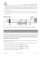


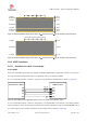
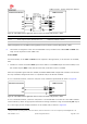

Table Of Contents
- Contents
- 1 System description
- 1.1 Overview
- 1.2 Architecture
- 1.3 Pin-out
- 1.4 Operating modes
- 1.5 Supply interfaces
- 1.5.1 Module supply input (VCC)
- 1.5.1.1 VCC supply requirements
- 1.5.1.2 VCC current consumption in 2G connected mode
- 1.5.1.3 VCC current consumption in 3G connected mode
- 1.5.1.4 VCC current consumption in LTE connected mode
- 1.5.1.5 VCC current consumption in cyclic low power idle mode / active mode
- 1.5.1.6 VCC current consumption in fixed active mode
- 1.5.2 Generic digital interfaces supply output (V_INT)
- 1.5.1 Module supply input (VCC)
- 1.6 System function interfaces
- 1.7 Antenna interfaces
- 1.8 SIM interfaces
- 1.9 Data communication interfaces
- 1.10 eMMC interface
- 1.11 Digital Audio interfaces
- 1.12 ADC interfaces
- 1.13 General Purpose Input/Output
- 1.14 Reserved pins (RSVD)
- 1.15 System features
- 1.15.1 Network indication
- 1.15.2 Jamming detection
- 1.15.3 IP modes of operation
- 1.15.4 Dual stack IPv4 and IPv6
- 1.15.5 Embedded TCP/IP and UDP/IP
- 1.15.6 Embedded FTP and FTPS
- 1.15.7 Embedded HTTP and HTTPS
- 1.15.8 SSL and TLS
- 1.15.9 Firmware update Over AT (FOAT)
- 1.15.10 Firmware update Over The Air (FOTA)
- 1.15.11 Power Saving
- 2 Design-in
- 2.1 Overview
- 2.2 Supply interfaces
- 2.2.1 Module supply (VCC)
- 2.2.1.1 General guidelines for VCC supply circuit selection and design
- 2.2.1.2 Guidelines for VCC supply circuit design using a switching regulator
- 2.2.1.3 Guidelines for VCC supply circuit design using a LDO linear regulator
- 2.2.1.4 Guidelines for VCC supply circuit design using a rechargeable battery
- 2.2.1.5 Guidelines for VCC supply circuit design using a primary battery
- 2.2.1.6 Additional guidelines for VCC supply circuit design
- 2.2.1.7 Guidelines for the external battery charging circuit
- 2.2.1.8 Guidelines for external charging and power path management circuit
- 2.2.1.9 Guidelines for removing VCC supply
- 2.2.1.10 Guidelines for VCC supply layout design
- 2.2.1.11 Guidelines for grounding layout design
- 2.2.2 Generic digital interfaces supply output (V_INT)
- 2.2.1 Module supply (VCC)
- 2.3 System functions interfaces
- 2.4 Antenna interface
- 2.5 SIM interfaces
- 2.6 Data communication interfaces
- 2.7 eMMC interface
- 2.8 Digital Audio interface
- 2.9 ADC interfaces
- 2.10 General Purpose Input/Output
- 2.11 Reserved pins (RSVD)
- 2.12 Module placement
- 2.13 Module footprint and paste mask
- 2.14 Thermal guidelines
- 2.15 Design-in checklist
- 3 Handling and soldering
- 4 Approvals
- 5 Product testing
- 6 FCC Notes
- Appendix
- Glossary
- Related documents
- Revision history
- Contact

TOBY-L3 series - System Integration Manual
TSD-19090601 - R13 System Integration Manual Page 97 of 143
D+
D–
GND
28
USB_D+
27
USB_D–
GND
USB 2.0 HOST
CONNECTOR
VBUS
D+
D–
GND
USB 2.0 DEVICE
PROCESSOR
TOBY-L3 series
VBUS
4
VUSB_DET
D1 D2 D3
C2
C2
28
USB_D+
27
USB_D–
GND
TOBY-L3 series
4
VUSB_DET
168
USB_ID
168
USB_ID
Boost
INOUT
Boost
IN
OUT
C1
5V
5V
C1
VCC
VCC
U1 U1
Figure 40: USB 2.0 interface application circuits, with TOBY-L3 series module acting as a USB host
Reference
Description
Part Number - Manufacturer
C1, C2
10 µF Capacitor Ceramic X7R 5750 15% 50 V
C5750X7R1H106MB - TDK
D1, D2, D3
Very Low Capacitance ESD Protection
PESD0402-140 - Tyco Electronics
U1
DC/DC Boost Regulator
Various Manufacturer
Table 34: Component for USB 2.0 interface application circuits, with TOBY-L3 series module acting as a USB host
2.6.1.2 Guidelines for USB layout design
The USB_D+/USB_D– lines require accurate layout design to achieve reliable signaling at the high speed
data rates (up to 480 Mbit/s) supported by the USB 2.0 interface.
The nominal characteristic impedance of the USB_D+/USB_D– lines is specified by the USB 2.0 specification
[4]. The most important parameter is the differential characteristic impedance applicable for the odd-mode
electromagnetic field, which should be as close as possible to 90 differential. Signal integrity may be
degraded if the PCB layout is not optimal, especially when the USB signaling lines are very long.
Use the following general routing guidelines to minimize signal quality problems:
Route the USB_D+ / USB_D– lines as a differential pair
Route the USB_D+ / USB_D– lines as short as possible
Ensure the differential characteristic impedance (Z
0
) is as close as possible to 90
Ensure the common mode characteristic impedance (Z
CM
) is as close as possible to 30
Consider design rules for the USB_D+ / USB_D– similar to RF transmission lines, these being coupled
differential micro-strip or buried stripline: avoid any stubs, abrupt change of layout, and route on clear
PCB area
Figure 41 and Figure 42 provide two examples of coplanar waveguide designs with differential characteristic
impedance close to 90 and common mode characteristic impedance close to 30 . The first transmission
line can be implemented for a 4-layer PCB stack-up herein illustrated; the second transmission line can be
implemented for a 2-layer PCB stack-up herein illustrated.