
Integration Manual
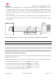


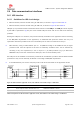
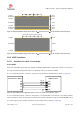

Table Of Contents
- Contents
- 1 System description
- 1.1 Overview
- 1.2 Architecture
- 1.3 Pin-out
- 1.4 Operating modes
- 1.5 Supply interfaces
- 1.5.1 Module supply input (VCC)
- 1.5.1.1 VCC supply requirements
- 1.5.1.2 VCC current consumption in 2G connected mode
- 1.5.1.3 VCC current consumption in 3G connected mode
- 1.5.1.4 VCC current consumption in LTE connected mode
- 1.5.1.5 VCC current consumption in cyclic low power idle mode / active mode
- 1.5.1.6 VCC current consumption in fixed active mode
- 1.5.2 Generic digital interfaces supply output (V_INT)
- 1.5.1 Module supply input (VCC)
- 1.6 System function interfaces
- 1.7 Antenna interfaces
- 1.8 SIM interfaces
- 1.9 Data communication interfaces
- 1.10 eMMC interface
- 1.11 Digital Audio interfaces
- 1.12 ADC interfaces
- 1.13 General Purpose Input/Output
- 1.14 Reserved pins (RSVD)
- 1.15 System features
- 1.15.1 Network indication
- 1.15.2 Jamming detection
- 1.15.3 IP modes of operation
- 1.15.4 Dual stack IPv4 and IPv6
- 1.15.5 Embedded TCP/IP and UDP/IP
- 1.15.6 Embedded FTP and FTPS
- 1.15.7 Embedded HTTP and HTTPS
- 1.15.8 SSL and TLS
- 1.15.9 Firmware update Over AT (FOAT)
- 1.15.10 Firmware update Over The Air (FOTA)
- 1.15.11 Power Saving
- 2 Design-in
- 2.1 Overview
- 2.2 Supply interfaces
- 2.2.1 Module supply (VCC)
- 2.2.1.1 General guidelines for VCC supply circuit selection and design
- 2.2.1.2 Guidelines for VCC supply circuit design using a switching regulator
- 2.2.1.3 Guidelines for VCC supply circuit design using a LDO linear regulator
- 2.2.1.4 Guidelines for VCC supply circuit design using a rechargeable battery
- 2.2.1.5 Guidelines for VCC supply circuit design using a primary battery
- 2.2.1.6 Additional guidelines for VCC supply circuit design
- 2.2.1.7 Guidelines for the external battery charging circuit
- 2.2.1.8 Guidelines for external charging and power path management circuit
- 2.2.1.9 Guidelines for removing VCC supply
- 2.2.1.10 Guidelines for VCC supply layout design
- 2.2.1.11 Guidelines for grounding layout design
- 2.2.2 Generic digital interfaces supply output (V_INT)
- 2.2.1 Module supply (VCC)
- 2.3 System functions interfaces
- 2.4 Antenna interface
- 2.5 SIM interfaces
- 2.6 Data communication interfaces
- 2.7 eMMC interface
- 2.8 Digital Audio interface
- 2.9 ADC interfaces
- 2.10 General Purpose Input/Output
- 2.11 Reserved pins (RSVD)
- 2.12 Module placement
- 2.13 Module footprint and paste mask
- 2.14 Thermal guidelines
- 2.15 Design-in checklist
- 3 Handling and soldering
- 4 Approvals
- 5 Product testing
- 6 FCC Notes
- Appendix
- Glossary
- Related documents
- Revision history
- Contact

TOBY-L3 series - System Integration Manual
TSD-19090601 - R13 System Integration Manual Page 93 of 143
Provide a 100 nF bypass capacitor (e.g. Murata GRM155R71C104K) at the SIM supply line close to the
relative pad of the SIM chip, to prevent digital noise.
Provide a bypass capacitor of about 22 pF to 47 pF (e.g. Murata GRM1555C1H470J) on each SIM line,
to prevent RF coupling especially when the RF antenna is placed closer than 10 - 30 cm from the SIM
lines.
Limit the capacitance and series resistance on each SIM signal to match the SIM requirements (23 ns is
the max rise time on the clock line, 1 µs is the max rise time on the data and reset lines).
TOBY-L3 series
VSIMx
SIMx_IO
SIMx_CLK
SIMx_RST
SIM CHIP
SIM Chip
Bottom View
(contacts side)
C1
VPP (C6)
VCC (C1)
IO (C7)
CLK (C3)
RST (C2)
GND (C5)
C2 C3 C5
U1
C4
2
8
3
6
7
1
C1 C5
C2 C6
C3 C7
C4 C8
8
7
6
5
1
2
3
4
Figure 37: Application circuits for the connection to a single solderable SIM chip, with SIM detection not implemented
Reference
Description
Part Number - Manufacturer
C1, C2, C3, C4
47 pF Capacitor Ceramic C0G 0402 5% 50 V
GRM1555C1H470JA01 - Murata
C5
100 nF Capacitor Ceramic X7R 0402 10% 16 V
GRM155R71C104KA01 - Murata
U1
SIM chip (M2M UICC Form Factor)
Various Manufacturers
Table 31: Example of components for the connection to a single solderable SIM chip, with SIM detection not implemented