
Integration Manual
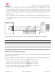


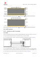
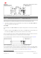

Table Of Contents
- Contents
- 1 System description
- 1.1 Overview
- 1.2 Architecture
- 1.3 Pin-out
- 1.4 Operating modes
- 1.5 Supply interfaces
- 1.5.1 Module supply input (VCC)
- 1.5.1.1 VCC supply requirements
- 1.5.1.2 VCC current consumption in 2G connected mode
- 1.5.1.3 VCC current consumption in 3G connected mode
- 1.5.1.4 VCC current consumption in LTE connected mode
- 1.5.1.5 VCC current consumption in cyclic low power idle mode / active mode
- 1.5.1.6 VCC current consumption in fixed active mode
- 1.5.2 Generic digital interfaces supply output (V_INT)
- 1.5.1 Module supply input (VCC)
- 1.6 System function interfaces
- 1.7 Antenna interfaces
- 1.8 SIM interfaces
- 1.9 Data communication interfaces
- 1.10 eMMC interface
- 1.11 Digital Audio interfaces
- 1.12 ADC interfaces
- 1.13 General Purpose Input/Output
- 1.14 Reserved pins (RSVD)
- 1.15 System features
- 1.15.1 Network indication
- 1.15.2 Jamming detection
- 1.15.3 IP modes of operation
- 1.15.4 Dual stack IPv4 and IPv6
- 1.15.5 Embedded TCP/IP and UDP/IP
- 1.15.6 Embedded FTP and FTPS
- 1.15.7 Embedded HTTP and HTTPS
- 1.15.8 SSL and TLS
- 1.15.9 Firmware update Over AT (FOAT)
- 1.15.10 Firmware update Over The Air (FOTA)
- 1.15.11 Power Saving
- 2 Design-in
- 2.1 Overview
- 2.2 Supply interfaces
- 2.2.1 Module supply (VCC)
- 2.2.1.1 General guidelines for VCC supply circuit selection and design
- 2.2.1.2 Guidelines for VCC supply circuit design using a switching regulator
- 2.2.1.3 Guidelines for VCC supply circuit design using a LDO linear regulator
- 2.2.1.4 Guidelines for VCC supply circuit design using a rechargeable battery
- 2.2.1.5 Guidelines for VCC supply circuit design using a primary battery
- 2.2.1.6 Additional guidelines for VCC supply circuit design
- 2.2.1.7 Guidelines for the external battery charging circuit
- 2.2.1.8 Guidelines for external charging and power path management circuit
- 2.2.1.9 Guidelines for removing VCC supply
- 2.2.1.10 Guidelines for VCC supply layout design
- 2.2.1.11 Guidelines for grounding layout design
- 2.2.2 Generic digital interfaces supply output (V_INT)
- 2.2.1 Module supply (VCC)
- 2.3 System functions interfaces
- 2.4 Antenna interface
- 2.5 SIM interfaces
- 2.6 Data communication interfaces
- 2.7 eMMC interface
- 2.8 Digital Audio interface
- 2.9 ADC interfaces
- 2.10 General Purpose Input/Output
- 2.11 Reserved pins (RSVD)
- 2.12 Module placement
- 2.13 Module footprint and paste mask
- 2.14 Thermal guidelines
- 2.15 Design-in checklist
- 3 Handling and soldering
- 4 Approvals
- 5 Product testing
- 6 FCC Notes
- Appendix
- Glossary
- Related documents
- Revision history
- Contact

TOBY-L3 series - System Integration Manual
TSD-19090601 - R13 System Integration Manual Page 92 of 143
Provide a very low capacitance (i.e. less than 10 pF) ESD protection (e.g. Tyco PESD0402-140) on each
externally accessible SIM line, close to each relative pad of the SIM connector. The ESD sensitivity rating
of the SIM interface pins is 1 kV (HBM). So that, according to EMC/ESD requirements of the custom
application, a higher protection level can be required if the lines are externally accessible on the
application device.
Limit the capacitance and series resistance on each SIM signal to match the SIM requirements (23 ns is
the maximum allowed rise time on the clock line, 1 µs is the maximum allowed rise time on the data
and reset lines).
TOBY-L3 series
VSIMx
SIMx_IO
SIMx_CLK
SIMx_RST
SIM CARD
HOLDER
C
5
C
6
C
7
C
1
C
2
C
3
SIM Card
Bottom View
(contacts side)
C1
VPP (C6)
VCC (C1)
IO (C7)
CLK (C3)
RST (C2)
GND (C5)
C2 C3 C5
J1
C4
D1 D2 D3 D4
C
8
C
4
Figure 36: Application circuits for the connection to a single removable SIM card, with SIM detection not implemented
Reference
Description
Part Number - Manufacturer
C1, C2, C3, C4
47 pF Capacitor Ceramic C0G 0402 5% 50 V
GRM1555C1H470JA01 - Murata
C5
100 nF Capacitor Ceramic X7R 0402 10% 16 V
GRM155R71C104KA01 - Murata
D1, D2, D3, D4
Very Low Capacitance ESD Protection
PESD0402-140 - Tyco Electronics
J1
SIM Card Holder, 6 p, without card presence switch
Various manufacturers, as C707 10M006 136 2 - Amphenol
Table 30: Example of components for the connection to a single removable SIM card, with SIM detection not implemented
Guidelines for single SIM chip connection
A solderable SIM chip (M2M UICC Form Factor) must be connected the SIM interface of the TOBY-L3 series
modules as shown in Figure 37.
Follow these guidelines to connect the module to a solderable SIM chip without SIM presence detection:
Connect the UICC / SIM contact C1 (VCC) to the VSIM pin of the module.
Connect the UICC / SIM contact C7 (I/O) to the SIM_IO pin of the module.
Connect the UICC / SIM contact C3 (CLK) to the SIM_CLK pin of the module.
Connect the UICC / SIM contact C2 (RST) to the SIM_RST pin of the module.
Connect the UICC / SIM contact C5 (GND) to ground.