
Integration Manual

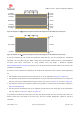


Table Of Contents
- Contents
- 1 System description
- 1.1 Overview
- 1.2 Architecture
- 1.3 Pin-out
- 1.4 Operating modes
- 1.5 Supply interfaces
- 1.5.1 Module supply input (VCC)
- 1.5.1.1 VCC supply requirements
- 1.5.1.2 VCC current consumption in 2G connected mode
- 1.5.1.3 VCC current consumption in 3G connected mode
- 1.5.1.4 VCC current consumption in LTE connected mode
- 1.5.1.5 VCC current consumption in cyclic low power idle mode / active mode
- 1.5.1.6 VCC current consumption in fixed active mode
- 1.5.2 Generic digital interfaces supply output (V_INT)
- 1.5.1 Module supply input (VCC)
- 1.6 System function interfaces
- 1.7 Antenna interfaces
- 1.8 SIM interfaces
- 1.9 Data communication interfaces
- 1.10 eMMC interface
- 1.11 Digital Audio interfaces
- 1.12 ADC interfaces
- 1.13 General Purpose Input/Output
- 1.14 Reserved pins (RSVD)
- 1.15 System features
- 1.15.1 Network indication
- 1.15.2 Jamming detection
- 1.15.3 IP modes of operation
- 1.15.4 Dual stack IPv4 and IPv6
- 1.15.5 Embedded TCP/IP and UDP/IP
- 1.15.6 Embedded FTP and FTPS
- 1.15.7 Embedded HTTP and HTTPS
- 1.15.8 SSL and TLS
- 1.15.9 Firmware update Over AT (FOAT)
- 1.15.10 Firmware update Over The Air (FOTA)
- 1.15.11 Power Saving
- 2 Design-in
- 2.1 Overview
- 2.2 Supply interfaces
- 2.2.1 Module supply (VCC)
- 2.2.1.1 General guidelines for VCC supply circuit selection and design
- 2.2.1.2 Guidelines for VCC supply circuit design using a switching regulator
- 2.2.1.3 Guidelines for VCC supply circuit design using a LDO linear regulator
- 2.2.1.4 Guidelines for VCC supply circuit design using a rechargeable battery
- 2.2.1.5 Guidelines for VCC supply circuit design using a primary battery
- 2.2.1.6 Additional guidelines for VCC supply circuit design
- 2.2.1.7 Guidelines for the external battery charging circuit
- 2.2.1.8 Guidelines for external charging and power path management circuit
- 2.2.1.9 Guidelines for removing VCC supply
- 2.2.1.10 Guidelines for VCC supply layout design
- 2.2.1.11 Guidelines for grounding layout design
- 2.2.2 Generic digital interfaces supply output (V_INT)
- 2.2.1 Module supply (VCC)
- 2.3 System functions interfaces
- 2.4 Antenna interface
- 2.5 SIM interfaces
- 2.6 Data communication interfaces
- 2.7 eMMC interface
- 2.8 Digital Audio interface
- 2.9 ADC interfaces
- 2.10 General Purpose Input/Output
- 2.11 Reserved pins (RSVD)
- 2.12 Module placement
- 2.13 Module footprint and paste mask
- 2.14 Thermal guidelines
- 2.15 Design-in checklist
- 3 Handling and soldering
- 4 Approvals
- 5 Product testing
- 6 FCC Notes
- Appendix
- Glossary
- Related documents
- Revision history
- Contact

TOBY-L3 series - System Integration Manual
TSD-19090601 - R13 System Integration Manual Page 90 of 143
2.4.2.2 Guidelines for ANT_DET layout design
The recommended layout for the primary antenna detection circuit to be provided on the application board
to achieve the primary antenna detection functionality, implementing the recommended schematic
illustrated in Figure 35 and Table 29, is explained here:
The ANT1 / ANT2 pins must be connected to the antenna connector by means of a 50 transmission
line, implementing the design guidelines described in section 2.4.1 and the recommendations of the
SMA connector manufacturer.
DC blocking capacitor at ANT1 / ANT2 pins (C2, C3) must be placed in series to the 50 RF line.
The ANT_DET pin must be connected to the 50 transmission line by means of a sense line.
Choke inductors in series at the ANT_DET pin (L1, L2) must be placed so that one pad is on the 50
transmission line and the other pad represents the start of the sense line to the ANT_DET pin.
The additional components (R1, C1 and D1) on the ANT_DET line must be placed as ESD protection.
2.5 SIM interfaces
2.5.1 Guidelines for SIM circuit design
TOBY-L3 series modules provide one SIM interface for the direct connection of external SIM cards/chips:
SIM interface (VSIM, SIM_IO, SIM_CLK, SIM_RST pins)
The ISO/IEC 7816, the ETSI TS 102 221 and the ETSI TS 102 671 specifications define the physical, electrical
and functional characteristics of Universal Integrated Circuit Cards (UICC), which contains the Subscriber
Identification Module (SIM) integrated circuit that securely stores all the information needed to identify and
authenticate subscribers over the LTE/3G/2G network.
Removable UICC / SIM card contact mapping is defined by ISO/IEC 7816 and ETSI TS 102 221:
Contact C1 = VCC (Supply) It must be connected to VSIM
Contact C2 = RST (Reset) It must be connected to SIM_RST
Contact C3 = CLK (Clock) It must be connected to SIM_CLK
Contact C4 = AUX1 (Auxiliary contact) It must be left not connected
Contact C5 = GND (Ground) It must be connected to GND
Contact C6 = VPP (Programming supply) It can be left not connected
Contact C7 = I/O (Data input/output) It must be connected to SIM_IO
Contact C8 = AUX2 (Auxiliary contact) It must be left not connected
A removable SIM card can have 6 contacts (C1, C2, C3, C5, C6, C7) or 8 contacts, also including the auxiliary
contacts C4 and C8. Only 5 contacts are required (C1, C2, C3, C5, C7) to be connected.