
Integration Manual

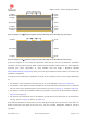


Table Of Contents
- Contents
- 1 System description
- 1.1 Overview
- 1.2 Architecture
- 1.3 Pin-out
- 1.4 Operating modes
- 1.5 Supply interfaces
- 1.5.1 Module supply input (VCC)
- 1.5.1.1 VCC supply requirements
- 1.5.1.2 VCC current consumption in 2G connected mode
- 1.5.1.3 VCC current consumption in 3G connected mode
- 1.5.1.4 VCC current consumption in LTE connected mode
- 1.5.1.5 VCC current consumption in cyclic low power idle mode / active mode
- 1.5.1.6 VCC current consumption in fixed active mode
- 1.5.2 Generic digital interfaces supply output (V_INT)
- 1.5.1 Module supply input (VCC)
- 1.6 System function interfaces
- 1.7 Antenna interfaces
- 1.8 SIM interfaces
- 1.9 Data communication interfaces
- 1.10 eMMC interface
- 1.11 Digital Audio interfaces
- 1.12 ADC interfaces
- 1.13 General Purpose Input/Output
- 1.14 Reserved pins (RSVD)
- 1.15 System features
- 1.15.1 Network indication
- 1.15.2 Jamming detection
- 1.15.3 IP modes of operation
- 1.15.4 Dual stack IPv4 and IPv6
- 1.15.5 Embedded TCP/IP and UDP/IP
- 1.15.6 Embedded FTP and FTPS
- 1.15.7 Embedded HTTP and HTTPS
- 1.15.8 SSL and TLS
- 1.15.9 Firmware update Over AT (FOAT)
- 1.15.10 Firmware update Over The Air (FOTA)
- 1.15.11 Power Saving
- 2 Design-in
- 2.1 Overview
- 2.2 Supply interfaces
- 2.2.1 Module supply (VCC)
- 2.2.1.1 General guidelines for VCC supply circuit selection and design
- 2.2.1.2 Guidelines for VCC supply circuit design using a switching regulator
- 2.2.1.3 Guidelines for VCC supply circuit design using a LDO linear regulator
- 2.2.1.4 Guidelines for VCC supply circuit design using a rechargeable battery
- 2.2.1.5 Guidelines for VCC supply circuit design using a primary battery
- 2.2.1.6 Additional guidelines for VCC supply circuit design
- 2.2.1.7 Guidelines for the external battery charging circuit
- 2.2.1.8 Guidelines for external charging and power path management circuit
- 2.2.1.9 Guidelines for removing VCC supply
- 2.2.1.10 Guidelines for VCC supply layout design
- 2.2.1.11 Guidelines for grounding layout design
- 2.2.2 Generic digital interfaces supply output (V_INT)
- 2.2.1 Module supply (VCC)
- 2.3 System functions interfaces
- 2.4 Antenna interface
- 2.5 SIM interfaces
- 2.6 Data communication interfaces
- 2.7 eMMC interface
- 2.8 Digital Audio interface
- 2.9 ADC interfaces
- 2.10 General Purpose Input/Output
- 2.11 Reserved pins (RSVD)
- 2.12 Module placement
- 2.13 Module footprint and paste mask
- 2.14 Thermal guidelines
- 2.15 Design-in checklist
- 3 Handling and soldering
- 4 Approvals
- 5 Product testing
- 6 FCC Notes
- Appendix
- Glossary
- Related documents
- Revision history
- Contact

TOBY-L3 series - System Integration Manual
TSD-19090601 - R13 System Integration Manual Page 86 of 143
Place the antennas far from sensitive analog systems or employ countermeasures to reduce EMC issues.
Take care of interaction between co-located RF systems since the LTE/3G/2G transmitted power may
interact or disturb the performance of companion systems.
Place the two LTE antennas providing low Envelope Correlation Coefficient (ECC) between the primary
(ANT1) and secondary (ANT2) antenna: the antenna 3D radiation patterns should have lobes in different
directions. The ECC between the primary and secondary antennas needs to be low enough to comply
with the radiated performance requirements specified by related certification schemes, as indicated in
Table 10.
Place the two LTE antennas providing enough high isolation (see Table 10) between the primary (ANT1)
and secondary (ANT2) antennas. The isolation depends on the distance between antennas (separation
of at least a quarter wavelength required for good isolation), antenna type (using antennas with different
polarization improves isolation), and the antenna 3D radiation patterns (uncorrelated patterns improve
isolation).
Examples of antennas
Table 26 lists some examples of possible internal on-board surface-mount antennas.
Manufacturer
Part Number
Product Name
Description
Taoglas
PA.710.A
Warrior
GSM / WCDMA / LTE SMD Antenna
698..960 MHz, 1710..2170 MHz, 2300..2400 MHz, 2490..2690 MHz
40.0 x 6.0 x 5.0 mm
Taoglas
PA.711.A
Warrior II
GSM / WCDMA / LTE SMD Antenna
Pairs with the Taoglas PA.710.A Warrior for LTE MIMO applications
698..960 MHz, 1710..2170 MHz, 2300..2400 MHz, 2490..2690 MHz
40.0 x 6.0 x 5.0 mm
Antenova
SR4L002
Lucida
GSM / WCDMA / LTE SMD Antenna
698..960 MHz, 1710..2170 MHz, 2300..2400 MHz, 2490..2690 MHz
35.0 x 8.5 x 3.2 mm
Table 26: Examples of internal surface-mount antennas
Table 27 lists some examples of possible internal off-board PCB-type antennas with cable and connector.
Manufacturer
Part Number
Product Name
Description
Taoglas
FXUB63.07.0150C
GSM / WCDMA / LTE PCB Antenna with cable and U.FL
698..960 MHz, 1575.42 MHz, 1710..2170 MHz, 2400..2690 MHz
96.0 x 21.0 mm
Taoglas
FXUB66.07.0150C
Maximus
GSM / WCDMA / LTE PCB Antenna with cable and U.FL
698..960 MHz, 1390..1435 MHz, 1575.42 MHz, 1710..2170 MHz,
2300..2700 MHz, 3400..3600 MHz, 4800..6000 MHz