
Integration Manual

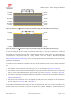


Table Of Contents
- Contents
- 1 System description
- 1.1 Overview
- 1.2 Architecture
- 1.3 Pin-out
- 1.4 Operating modes
- 1.5 Supply interfaces
- 1.5.1 Module supply input (VCC)
- 1.5.1.1 VCC supply requirements
- 1.5.1.2 VCC current consumption in 2G connected mode
- 1.5.1.3 VCC current consumption in 3G connected mode
- 1.5.1.4 VCC current consumption in LTE connected mode
- 1.5.1.5 VCC current consumption in cyclic low power idle mode / active mode
- 1.5.1.6 VCC current consumption in fixed active mode
- 1.5.2 Generic digital interfaces supply output (V_INT)
- 1.5.1 Module supply input (VCC)
- 1.6 System function interfaces
- 1.7 Antenna interfaces
- 1.8 SIM interfaces
- 1.9 Data communication interfaces
- 1.10 eMMC interface
- 1.11 Digital Audio interfaces
- 1.12 ADC interfaces
- 1.13 General Purpose Input/Output
- 1.14 Reserved pins (RSVD)
- 1.15 System features
- 1.15.1 Network indication
- 1.15.2 Jamming detection
- 1.15.3 IP modes of operation
- 1.15.4 Dual stack IPv4 and IPv6
- 1.15.5 Embedded TCP/IP and UDP/IP
- 1.15.6 Embedded FTP and FTPS
- 1.15.7 Embedded HTTP and HTTPS
- 1.15.8 SSL and TLS
- 1.15.9 Firmware update Over AT (FOAT)
- 1.15.10 Firmware update Over The Air (FOTA)
- 1.15.11 Power Saving
- 2 Design-in
- 2.1 Overview
- 2.2 Supply interfaces
- 2.2.1 Module supply (VCC)
- 2.2.1.1 General guidelines for VCC supply circuit selection and design
- 2.2.1.2 Guidelines for VCC supply circuit design using a switching regulator
- 2.2.1.3 Guidelines for VCC supply circuit design using a LDO linear regulator
- 2.2.1.4 Guidelines for VCC supply circuit design using a rechargeable battery
- 2.2.1.5 Guidelines for VCC supply circuit design using a primary battery
- 2.2.1.6 Additional guidelines for VCC supply circuit design
- 2.2.1.7 Guidelines for the external battery charging circuit
- 2.2.1.8 Guidelines for external charging and power path management circuit
- 2.2.1.9 Guidelines for removing VCC supply
- 2.2.1.10 Guidelines for VCC supply layout design
- 2.2.1.11 Guidelines for grounding layout design
- 2.2.2 Generic digital interfaces supply output (V_INT)
- 2.2.1 Module supply (VCC)
- 2.3 System functions interfaces
- 2.4 Antenna interface
- 2.5 SIM interfaces
- 2.6 Data communication interfaces
- 2.7 eMMC interface
- 2.8 Digital Audio interface
- 2.9 ADC interfaces
- 2.10 General Purpose Input/Output
- 2.11 Reserved pins (RSVD)
- 2.12 Module placement
- 2.13 Module footprint and paste mask
- 2.14 Thermal guidelines
- 2.15 Design-in checklist
- 3 Handling and soldering
- 4 Approvals
- 5 Product testing
- 6 FCC Notes
- Appendix
- Glossary
- Related documents
- Revision history
- Contact

TOBY-L3 series - System Integration Manual
TSD-19090601 - R13 System Integration Manual Page 85 of 143
Guidelines for RF termination design
RF terminations must provide a characteristic impedance of 50 as well as the RF transmission lines up to
the RF terminations themselves, to match the characteristic impedance of the ANT1 / ANT2 ports of the
modules.
However, real antennas do not have a perfect 50 load on all the supported frequency bands. Therefore,
to reduce as much as possible any performance degradation due to antennas mismatch, the RF terminations
must provide optimal return loss (or VSWR) figures over all the operating frequencies, as summarized in
Table 8 and Table 9.
If external antennas are used, the antenna connectors represent the RF termination on the PCB:
Use suitable 50 connectors providing a correct PCB-to-RF-cable transition.
Strictly follow the connector manufacturer’s recommended layout, for example:
o SMA pin-through-hole connectors require GND keep-out (i.e. clearance, a void area) on all layers
around the central pin up to the annular pads of the four GND posts, as shown in Figure 34.
o U.FL surface-mounted connectors require no conductive traces (i.e. clearance, a void area) in the area
below the connector between the GND land pads.
Cut out the GND layer under RF connectors and close to buried vias, in order to remove stray capacitance
and thus keep the RF line 50 , e.g. the active pad of U.FL connectors needs to have a GND keep-out
(i.e. clearance, a void area) at least on the first inner layer to reduce parasitic capacitance to ground.
If integrated antennas are used, the RF terminations are represented by the integrated antennas themselves.
The following guidelines should be followed:
Use antennas designed by an antenna manufacturer, providing the best possible return loss (or VSWR).
Provide a ground plane large enough according to the relative integrated antenna requirements. The
ground plane of the application PCB can be reduced down to a minimum size that must be similar to
one quarter of a wavelength of the minimum frequency that must be radiated. As a numerical example,
Frequency = 750 MHz Wavelength = 40 cm Minimum GND plane size = 10 cm
It is highly recommended to strictly follow the detailed and specific guidelines provided by the antenna
manufacturer regarding correct installation and deployment of the antenna system, including PCB layout
and matching circuitry.
Further to the custom PCB and product restrictions, antennas may require a tuning to comply with all
the applicable required certification schemes. It is recommended to consult the antenna manufacturer
for the design-in guidelines for the antenna matching relative to the custom application.
Additionally, these recommendations regarding the antenna system placement must be followed:
Do not place antennas within a closed metal case.
Do not place the antennas in close vicinity to the end user since the emitted radiation in human tissue
is limited by regulatory requirements.