
Integration Manual

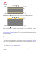


Table Of Contents
- Contents
- 1 System description
- 1.1 Overview
- 1.2 Architecture
- 1.3 Pin-out
- 1.4 Operating modes
- 1.5 Supply interfaces
- 1.5.1 Module supply input (VCC)
- 1.5.1.1 VCC supply requirements
- 1.5.1.2 VCC current consumption in 2G connected mode
- 1.5.1.3 VCC current consumption in 3G connected mode
- 1.5.1.4 VCC current consumption in LTE connected mode
- 1.5.1.5 VCC current consumption in cyclic low power idle mode / active mode
- 1.5.1.6 VCC current consumption in fixed active mode
- 1.5.2 Generic digital interfaces supply output (V_INT)
- 1.5.1 Module supply input (VCC)
- 1.6 System function interfaces
- 1.7 Antenna interfaces
- 1.8 SIM interfaces
- 1.9 Data communication interfaces
- 1.10 eMMC interface
- 1.11 Digital Audio interfaces
- 1.12 ADC interfaces
- 1.13 General Purpose Input/Output
- 1.14 Reserved pins (RSVD)
- 1.15 System features
- 1.15.1 Network indication
- 1.15.2 Jamming detection
- 1.15.3 IP modes of operation
- 1.15.4 Dual stack IPv4 and IPv6
- 1.15.5 Embedded TCP/IP and UDP/IP
- 1.15.6 Embedded FTP and FTPS
- 1.15.7 Embedded HTTP and HTTPS
- 1.15.8 SSL and TLS
- 1.15.9 Firmware update Over AT (FOAT)
- 1.15.10 Firmware update Over The Air (FOTA)
- 1.15.11 Power Saving
- 2 Design-in
- 2.1 Overview
- 2.2 Supply interfaces
- 2.2.1 Module supply (VCC)
- 2.2.1.1 General guidelines for VCC supply circuit selection and design
- 2.2.1.2 Guidelines for VCC supply circuit design using a switching regulator
- 2.2.1.3 Guidelines for VCC supply circuit design using a LDO linear regulator
- 2.2.1.4 Guidelines for VCC supply circuit design using a rechargeable battery
- 2.2.1.5 Guidelines for VCC supply circuit design using a primary battery
- 2.2.1.6 Additional guidelines for VCC supply circuit design
- 2.2.1.7 Guidelines for the external battery charging circuit
- 2.2.1.8 Guidelines for external charging and power path management circuit
- 2.2.1.9 Guidelines for removing VCC supply
- 2.2.1.10 Guidelines for VCC supply layout design
- 2.2.1.11 Guidelines for grounding layout design
- 2.2.2 Generic digital interfaces supply output (V_INT)
- 2.2.1 Module supply (VCC)
- 2.3 System functions interfaces
- 2.4 Antenna interface
- 2.5 SIM interfaces
- 2.6 Data communication interfaces
- 2.7 eMMC interface
- 2.8 Digital Audio interface
- 2.9 ADC interfaces
- 2.10 General Purpose Input/Output
- 2.11 Reserved pins (RSVD)
- 2.12 Module placement
- 2.13 Module footprint and paste mask
- 2.14 Thermal guidelines
- 2.15 Design-in checklist
- 3 Handling and soldering
- 4 Approvals
- 5 Product testing
- 6 FCC Notes
- Appendix
- Glossary
- Related documents
- Revision history
- Contact

TOBY-L3 series - System Integration Manual
TSD-19090601 - R13 System Integration Manual Page 84 of 143
Additionally to the 50 impedance, the following guidelines are recommended for transmission line design:
Minimize the transmission line length: the insertion loss should be minimized as much as possible, in
the order of a few tenths of a dB.
Add GND keep-out (i.e. clearance, a void area) on buried metal layers below any pad of a component
present on the RF transmission lines, if the top-layer to buried layer dielectric thickness is below 200 µm,
to reduce parasitic capacitance to ground.
The transmission lines width and spacing to GND must be uniform and routed as smoothly as possible:
avoid abrupt changes of width and spacing to GND.
Add GND stitching vias around the transmission lines, as shown in Figure 34.
Ensure a solid metal connection of the adjacent metal layer on the PCB stack-up to the main ground
layer, providing enough vias on the adjacent metal layer, as shown in Figure 34.
Route RF transmission lines far from any noise source (as switching supplies and digital lines) and from
any sensitive circuit (as USB).
Avoid stubs on the transmission lines.
Avoid signal routing in parallel to the transmission lines or crossing the transmission lines on a buried
metal layer.
Do not route the microstrip lines below discrete components or other mechanics placed on the top
layer.
An example of a suitable RF circuit design is illustrated in Figure 34. In this case, the ANT1 and ANT2 pins
are directly connected to SMA connectors by means of suitable 50 transmission lines, designed with a
suitable layout.
SMA Connector
Primary Antenna
SMA Connector
Secondary Antenna
TOBY-L3
Figure 34: Example of the circuit and layout for antenna RF circuits on the application board