
Integration Manual

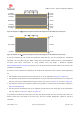


Table Of Contents
- Contents
- 1 System description
- 1.1 Overview
- 1.2 Architecture
- 1.3 Pin-out
- 1.4 Operating modes
- 1.5 Supply interfaces
- 1.5.1 Module supply input (VCC)
- 1.5.1.1 VCC supply requirements
- 1.5.1.2 VCC current consumption in 2G connected mode
- 1.5.1.3 VCC current consumption in 3G connected mode
- 1.5.1.4 VCC current consumption in LTE connected mode
- 1.5.1.5 VCC current consumption in cyclic low power idle mode / active mode
- 1.5.1.6 VCC current consumption in fixed active mode
- 1.5.2 Generic digital interfaces supply output (V_INT)
- 1.5.1 Module supply input (VCC)
- 1.6 System function interfaces
- 1.7 Antenna interfaces
- 1.8 SIM interfaces
- 1.9 Data communication interfaces
- 1.10 eMMC interface
- 1.11 Digital Audio interfaces
- 1.12 ADC interfaces
- 1.13 General Purpose Input/Output
- 1.14 Reserved pins (RSVD)
- 1.15 System features
- 1.15.1 Network indication
- 1.15.2 Jamming detection
- 1.15.3 IP modes of operation
- 1.15.4 Dual stack IPv4 and IPv6
- 1.15.5 Embedded TCP/IP and UDP/IP
- 1.15.6 Embedded FTP and FTPS
- 1.15.7 Embedded HTTP and HTTPS
- 1.15.8 SSL and TLS
- 1.15.9 Firmware update Over AT (FOAT)
- 1.15.10 Firmware update Over The Air (FOTA)
- 1.15.11 Power Saving
- 2 Design-in
- 2.1 Overview
- 2.2 Supply interfaces
- 2.2.1 Module supply (VCC)
- 2.2.1.1 General guidelines for VCC supply circuit selection and design
- 2.2.1.2 Guidelines for VCC supply circuit design using a switching regulator
- 2.2.1.3 Guidelines for VCC supply circuit design using a LDO linear regulator
- 2.2.1.4 Guidelines for VCC supply circuit design using a rechargeable battery
- 2.2.1.5 Guidelines for VCC supply circuit design using a primary battery
- 2.2.1.6 Additional guidelines for VCC supply circuit design
- 2.2.1.7 Guidelines for the external battery charging circuit
- 2.2.1.8 Guidelines for external charging and power path management circuit
- 2.2.1.9 Guidelines for removing VCC supply
- 2.2.1.10 Guidelines for VCC supply layout design
- 2.2.1.11 Guidelines for grounding layout design
- 2.2.2 Generic digital interfaces supply output (V_INT)
- 2.2.1 Module supply (VCC)
- 2.3 System functions interfaces
- 2.4 Antenna interface
- 2.5 SIM interfaces
- 2.6 Data communication interfaces
- 2.7 eMMC interface
- 2.8 Digital Audio interface
- 2.9 ADC interfaces
- 2.10 General Purpose Input/Output
- 2.11 Reserved pins (RSVD)
- 2.12 Module placement
- 2.13 Module footprint and paste mask
- 2.14 Thermal guidelines
- 2.15 Design-in checklist
- 3 Handling and soldering
- 4 Approvals
- 5 Product testing
- 6 FCC Notes
- Appendix
- Glossary
- Related documents
- Revision history
- Contact

TOBY-L3 series - System Integration Manual
TSD-19090601 - R13 System Integration Manual Page 83 of 143
35 um
35 um
35 um
35 um
270 um
270 um
760 um
L1 Copper
L3 Copper
L2 Copper
L4 Copper
FR-4 dielectric
FR-4 dielectric
FR-4 dielectric
380 um 500 um500 um
Figure 32: Example of a 50 coplanar waveguide transmission line design for the described 4-layer board layup
35 um
35 um
1510 um
L2 Copper
L1 Copper
FR-4 dielectric
1200 um 400 um400 um
Figure 33: Example of a 50 coplanar waveguide transmission line design for the described 2-layer board layup
If the two examples do not match the application PCB stack-up, the 50 characteristic impedance
calculation can be made using the HFSS commercial finite element method solver for electromagnetic
structures from Ansys Corporation, or using freeware tools like Avago / Broadcom AppCAD
(https://www.broadcom.com/appcad), taking care of the approximation formulas used by the tools for the
impedance computation.
To achieve a 50 characteristic impedance, the width of the transmission line must be chosen depending
on:
the thickness of the transmission line itself (e.g. 35 µm in the examples of Figure 32 / Figure 33)
the thickness of the dielectric material between the top layer (where the transmission line is routed) and
the inner closer layer implementing the ground plane (e.g. 270 µm in Figure 32, 1510 µm in Figure 33)
the dielectric constant of the dielectric material (e.g. dielectric constant of the FR-4 dielectric material in
Figure 32 and Figure 33)
the gap from the transmission line to the adjacent ground plane on the same layer of the transmission
line (e.g. 500 µm in Figure 32, 400 µm in Figure 33)
If the distance between the transmission line and the adjacent GND area (on the same layer) does not
exceed 5 times the track width of the micro strip, use the “Coplanar Waveguide” model for the 50
calculation.