
Integration Manual

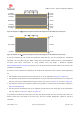


Table Of Contents
- Contents
- 1 System description
- 1.1 Overview
- 1.2 Architecture
- 1.3 Pin-out
- 1.4 Operating modes
- 1.5 Supply interfaces
- 1.5.1 Module supply input (VCC)
- 1.5.1.1 VCC supply requirements
- 1.5.1.2 VCC current consumption in 2G connected mode
- 1.5.1.3 VCC current consumption in 3G connected mode
- 1.5.1.4 VCC current consumption in LTE connected mode
- 1.5.1.5 VCC current consumption in cyclic low power idle mode / active mode
- 1.5.1.6 VCC current consumption in fixed active mode
- 1.5.2 Generic digital interfaces supply output (V_INT)
- 1.5.1 Module supply input (VCC)
- 1.6 System function interfaces
- 1.7 Antenna interfaces
- 1.8 SIM interfaces
- 1.9 Data communication interfaces
- 1.10 eMMC interface
- 1.11 Digital Audio interfaces
- 1.12 ADC interfaces
- 1.13 General Purpose Input/Output
- 1.14 Reserved pins (RSVD)
- 1.15 System features
- 1.15.1 Network indication
- 1.15.2 Jamming detection
- 1.15.3 IP modes of operation
- 1.15.4 Dual stack IPv4 and IPv6
- 1.15.5 Embedded TCP/IP and UDP/IP
- 1.15.6 Embedded FTP and FTPS
- 1.15.7 Embedded HTTP and HTTPS
- 1.15.8 SSL and TLS
- 1.15.9 Firmware update Over AT (FOAT)
- 1.15.10 Firmware update Over The Air (FOTA)
- 1.15.11 Power Saving
- 2 Design-in
- 2.1 Overview
- 2.2 Supply interfaces
- 2.2.1 Module supply (VCC)
- 2.2.1.1 General guidelines for VCC supply circuit selection and design
- 2.2.1.2 Guidelines for VCC supply circuit design using a switching regulator
- 2.2.1.3 Guidelines for VCC supply circuit design using a LDO linear regulator
- 2.2.1.4 Guidelines for VCC supply circuit design using a rechargeable battery
- 2.2.1.5 Guidelines for VCC supply circuit design using a primary battery
- 2.2.1.6 Additional guidelines for VCC supply circuit design
- 2.2.1.7 Guidelines for the external battery charging circuit
- 2.2.1.8 Guidelines for external charging and power path management circuit
- 2.2.1.9 Guidelines for removing VCC supply
- 2.2.1.10 Guidelines for VCC supply layout design
- 2.2.1.11 Guidelines for grounding layout design
- 2.2.2 Generic digital interfaces supply output (V_INT)
- 2.2.1 Module supply (VCC)
- 2.3 System functions interfaces
- 2.4 Antenna interface
- 2.5 SIM interfaces
- 2.6 Data communication interfaces
- 2.7 eMMC interface
- 2.8 Digital Audio interface
- 2.9 ADC interfaces
- 2.10 General Purpose Input/Output
- 2.11 Reserved pins (RSVD)
- 2.12 Module placement
- 2.13 Module footprint and paste mask
- 2.14 Thermal guidelines
- 2.15 Design-in checklist
- 3 Handling and soldering
- 4 Approvals
- 5 Product testing
- 6 FCC Notes
- Appendix
- Glossary
- Related documents
- Revision history
- Contact

TOBY-L3 series - System Integration Manual
TSD-19090601 - R13 System Integration Manual Page 81 of 143
can be radiated. Therefore, the ground plane can be reduced down to a minimum size that should
be similar to the quarter of the wavelength of the minimum frequency that must be radiated, given
that the orientation of the ground plane relative to the antenna element must be considered.
The isolation between the primary and the secondary antennas must be as high as possible and the
correlation between the 3D radiation patterns of the two antennas must be as low as possible. In
general, a separation of at least a quarter wavelength between the two antennas is required to
achieve a good isolation and low pattern correlation.
As a numerical example, the physical restriction to the PCB design can be considered as following:
Frequency = 750 MHz Wavelength = 40 cm Minimum GND plane size = 10 cm
o Radiation performance depends on the whole PCB and antenna system design, including product
mechanical design and usage. Antennas should be selected with optimal radiating performance in the
operating bands according to the mechanical specifications of the PCB and the whole product.
o It is recommended to select a pair of custom antennas designed by an antennas’ manufacturer if the
required ground plane dimensions are very small (less than 6.5 cm long and 4 cm wide). The antenna
design process should begin at the start of the whole product design process.
o It is highly recommended to strictly follow the detailed and specific guidelines provided by the
antenna manufacturer regarding correct installation and deployment of the antenna system, including
PCB layout and matching circuitry.
o Further to the custom PCB and product restrictions, antennas may require tuning to obtain the
required performance for compliance with all the applicable required certification schemes. It is
recommended to consult the antenna manufacturer for the design-in guidelines for antenna matching
relative to the custom application.
In both cases, selecting external or internal antennas, these recommendations should be observed:
Select antennas providing optimal return loss (VSWR) figures over all the operating frequencies.
Select antennas providing optimal efficiency figures over all the operating frequencies.
Select antennas providing similar efficiency for both the primary (ANT1) and the secondary (ANT2)
antenna.
Select antennas providing appropriate maximum gain figures (i.e. combined antenna directivity and
efficiency figures) so that the in-band radiation intensity does not exceed the regulatory limits specified
by local authorities.
Select antennas capable of providing a low Envelope Correlation Coefficient between the primary (ANT1)
and the secondary (ANT2) antenna: the 3D antenna radiation patterns should have lobes in different
directions.
2.4.1.2 Guidelines for antenna RF interface design
Guidelines for ANT1 / ANT2 pins RF connection design