
Integration Manual
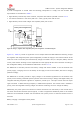


Table Of Contents
- Contents
- 1 System description
- 1.1 Overview
- 1.2 Architecture
- 1.3 Pin-out
- 1.4 Operating modes
- 1.5 Supply interfaces
- 1.5.1 Module supply input (VCC)
- 1.5.1.1 VCC supply requirements
- 1.5.1.2 VCC current consumption in 2G connected mode
- 1.5.1.3 VCC current consumption in 3G connected mode
- 1.5.1.4 VCC current consumption in LTE connected mode
- 1.5.1.5 VCC current consumption in cyclic low power idle mode / active mode
- 1.5.1.6 VCC current consumption in fixed active mode
- 1.5.2 Generic digital interfaces supply output (V_INT)
- 1.5.1 Module supply input (VCC)
- 1.6 System function interfaces
- 1.7 Antenna interfaces
- 1.8 SIM interfaces
- 1.9 Data communication interfaces
- 1.10 eMMC interface
- 1.11 Digital Audio interfaces
- 1.12 ADC interfaces
- 1.13 General Purpose Input/Output
- 1.14 Reserved pins (RSVD)
- 1.15 System features
- 1.15.1 Network indication
- 1.15.2 Jamming detection
- 1.15.3 IP modes of operation
- 1.15.4 Dual stack IPv4 and IPv6
- 1.15.5 Embedded TCP/IP and UDP/IP
- 1.15.6 Embedded FTP and FTPS
- 1.15.7 Embedded HTTP and HTTPS
- 1.15.8 SSL and TLS
- 1.15.9 Firmware update Over AT (FOAT)
- 1.15.10 Firmware update Over The Air (FOTA)
- 1.15.11 Power Saving
- 2 Design-in
- 2.1 Overview
- 2.2 Supply interfaces
- 2.2.1 Module supply (VCC)
- 2.2.1.1 General guidelines for VCC supply circuit selection and design
- 2.2.1.2 Guidelines for VCC supply circuit design using a switching regulator
- 2.2.1.3 Guidelines for VCC supply circuit design using a LDO linear regulator
- 2.2.1.4 Guidelines for VCC supply circuit design using a rechargeable battery
- 2.2.1.5 Guidelines for VCC supply circuit design using a primary battery
- 2.2.1.6 Additional guidelines for VCC supply circuit design
- 2.2.1.7 Guidelines for the external battery charging circuit
- 2.2.1.8 Guidelines for external charging and power path management circuit
- 2.2.1.9 Guidelines for removing VCC supply
- 2.2.1.10 Guidelines for VCC supply layout design
- 2.2.1.11 Guidelines for grounding layout design
- 2.2.2 Generic digital interfaces supply output (V_INT)
- 2.2.1 Module supply (VCC)
- 2.3 System functions interfaces
- 2.4 Antenna interface
- 2.5 SIM interfaces
- 2.6 Data communication interfaces
- 2.7 eMMC interface
- 2.8 Digital Audio interface
- 2.9 ADC interfaces
- 2.10 General Purpose Input/Output
- 2.11 Reserved pins (RSVD)
- 2.12 Module placement
- 2.13 Module footprint and paste mask
- 2.14 Thermal guidelines
- 2.15 Design-in checklist
- 3 Handling and soldering
- 4 Approvals
- 5 Product testing
- 6 FCC Notes
- Appendix
- Glossary
- Related documents
- Revision history
- Contact

TOBY-L3 series - System Integration Manual
TSD-19090601 - R13 System Integration Manual Page 80 of 143
2.4 Antenna interface
TOBY-L3 series modules provide two RF interfaces for connecting the external antennas:
The ANT1 pin represents the primary RF input/output for RF signals transmission and reception.
The ANT2 pin represents the secondary RF input for MIMO and Rx diversity RF signals reception.
Both the ANT1 and the ANT2 pins have a nominal characteristic impedance of 50 and must be connected
to the related antenna through a 50 transmission line to allow correct transmission / reception of RF
signals.
☞ Two antennas (one connected to ANT1 pin and one connected to ANT2 pin) must be used to support
the MIMO and Rx diversity configurations. This is a required feature for LTE category 4 User Equipment
(up to 150 Mbit/s Down-Link data rate) according to the 3GPP specifications.
2.4.1 Antenna RF interfaces (ANT1 / ANT2)
2.4.1.1 General guidelines for antenna selection and design
The antenna is the most critical component to be evaluated. Designers must take care of the antennas from
all perspectives at the very start of the design phase when the physical dimensions of the application board
are under analysis/decision, since the RF compliance of the device integrating TOBY-L3 series modules with
all the applicable required certification schemes depends on the antenna radiating performance.
LTE/3G/2G antennas are typically available in the types of linear monopole or PCB antennas such as patches
or ceramic SMT elements.
External antennas (e.g. linear monopole)
o External antennas basically do not imply a physical restriction to the design of the PCB where the
TOBY-L3 series module is mounted.
o The radiation performance mainly depends on the antennas. It is required to select antennas with
optimal radiating performance in the operating bands.
o RF cables should be carefully selected to have minimum insertion losses. Additional insertion loss will
be introduced by low quality or long cable. Large insertion loss reduces both transmit and receive
radiation performance.
o A high quality 50 RF connector provides suitable PCB-to-RF-cable transition. It is recommended to
strictly follow the layout and cable termination guidelines provided by the connector manufacturer.
Integrated antennas (e.g. patch-like antennas):
o Internal integrated antennas imply a physical restriction to the design of the PCB:
An integrated antenna excites RF currents on its counterpoise, typically the PCB ground plane of
the device that becomes part of the antenna: its dimension defines the minimum frequency that