
Integration Manual
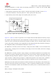


Table Of Contents
- Contents
- 1 System description
- 1.1 Overview
- 1.2 Architecture
- 1.3 Pin-out
- 1.4 Operating modes
- 1.5 Supply interfaces
- 1.5.1 Module supply input (VCC)
- 1.5.1.1 VCC supply requirements
- 1.5.1.2 VCC current consumption in 2G connected mode
- 1.5.1.3 VCC current consumption in 3G connected mode
- 1.5.1.4 VCC current consumption in LTE connected mode
- 1.5.1.5 VCC current consumption in cyclic low power idle mode / active mode
- 1.5.1.6 VCC current consumption in fixed active mode
- 1.5.2 Generic digital interfaces supply output (V_INT)
- 1.5.1 Module supply input (VCC)
- 1.6 System function interfaces
- 1.7 Antenna interfaces
- 1.8 SIM interfaces
- 1.9 Data communication interfaces
- 1.10 eMMC interface
- 1.11 Digital Audio interfaces
- 1.12 ADC interfaces
- 1.13 General Purpose Input/Output
- 1.14 Reserved pins (RSVD)
- 1.15 System features
- 1.15.1 Network indication
- 1.15.2 Jamming detection
- 1.15.3 IP modes of operation
- 1.15.4 Dual stack IPv4 and IPv6
- 1.15.5 Embedded TCP/IP and UDP/IP
- 1.15.6 Embedded FTP and FTPS
- 1.15.7 Embedded HTTP and HTTPS
- 1.15.8 SSL and TLS
- 1.15.9 Firmware update Over AT (FOAT)
- 1.15.10 Firmware update Over The Air (FOTA)
- 1.15.11 Power Saving
- 2 Design-in
- 2.1 Overview
- 2.2 Supply interfaces
- 2.2.1 Module supply (VCC)
- 2.2.1.1 General guidelines for VCC supply circuit selection and design
- 2.2.1.2 Guidelines for VCC supply circuit design using a switching regulator
- 2.2.1.3 Guidelines for VCC supply circuit design using a LDO linear regulator
- 2.2.1.4 Guidelines for VCC supply circuit design using a rechargeable battery
- 2.2.1.5 Guidelines for VCC supply circuit design using a primary battery
- 2.2.1.6 Additional guidelines for VCC supply circuit design
- 2.2.1.7 Guidelines for the external battery charging circuit
- 2.2.1.8 Guidelines for external charging and power path management circuit
- 2.2.1.9 Guidelines for removing VCC supply
- 2.2.1.10 Guidelines for VCC supply layout design
- 2.2.1.11 Guidelines for grounding layout design
- 2.2.2 Generic digital interfaces supply output (V_INT)
- 2.2.1 Module supply (VCC)
- 2.3 System functions interfaces
- 2.4 Antenna interface
- 2.5 SIM interfaces
- 2.6 Data communication interfaces
- 2.7 eMMC interface
- 2.8 Digital Audio interface
- 2.9 ADC interfaces
- 2.10 General Purpose Input/Output
- 2.11 Reserved pins (RSVD)
- 2.12 Module placement
- 2.13 Module footprint and paste mask
- 2.14 Thermal guidelines
- 2.15 Design-in checklist
- 3 Handling and soldering
- 4 Approvals
- 5 Product testing
- 6 FCC Notes
- Appendix
- Glossary
- Related documents
- Revision history
- Contact

TOBY-L3 series - System Integration Manual
TSD-19090601 - R13 System Integration Manual Page 76 of 143
Pull-up SIM detection signal (see section 2.5 for more details)
Supply voltage translators to connect 1.8 V module generic digital interfaces to 3.0 V devices (e.g. see
section 2.6.1 for more details)
Pull-up DDC (I
2
C) interface signals (see section 2.6.4 for more details)
Supply a 1.8 V u-blox GNSS device (see section 2.6.4 for more details)
Enable external voltage regulators providing supply for external devices, as linear LDO regulators
providing the 3.3 V / 1.8 V supply rails for a u-blox EMMY-W1 series module (see section 2.6.5 for more
details)
Supply an external device as an external 1.8 V audio codec (see section 2.8 for more details)
The V_INT supply output pin provides internal short circuit protection to limit the start-up current and
protect the device in short circuit situations. No additional external short circuit protection is required.
☞ Do not apply loads which might exceed the limit for the maximum available current from V_INT supply
(see TOBY-L3 series Data Sheet [1]) as this can cause malfunctions in the internal circuitry.
☞ Since the V_INT supply is generated by an internal switching step-down regulator (the V_INT voltage
ripple can range as specified in the TOBY-L3 series Data Sheet [1]), it is not recommended to supply
sensitive analog circuitry without adequate filtering for digital noise.
☞ V_INT can only be used as an output: do not connect any external supply source on V_INT.
☞ The ESD sensitivity rating of the V_INT supply pin is 1 kV (Human Body Model according to JESD22-
A114). A higher protection level could be required if the line is externally accessible and it can be
achieved by mounting an ESD protection (e.g. EPCOS CA05P4S14THSG varistor array) close to the
accessible point.
☞ It is recommended to monitor the V_INT pin to sense the end of the internal switch-off sequence of
TOBY-L3 series modules: the VCC supply can be removed only after V_INT goes low
☞ It is recommended to provide direct access to the V_INT pin on the application board by means of an
accessible test point directly connected to the V_INT pin, for diagnostic purposes.