
Integration Manual


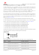


Table Of Contents
- Contents
- 1 System description
- 1.1 Overview
- 1.2 Architecture
- 1.3 Pin-out
- 1.4 Operating modes
- 1.5 Supply interfaces
- 1.5.1 Module supply input (VCC)
- 1.5.1.1 VCC supply requirements
- 1.5.1.2 VCC current consumption in 2G connected mode
- 1.5.1.3 VCC current consumption in 3G connected mode
- 1.5.1.4 VCC current consumption in LTE connected mode
- 1.5.1.5 VCC current consumption in cyclic low power idle mode / active mode
- 1.5.1.6 VCC current consumption in fixed active mode
- 1.5.2 Generic digital interfaces supply output (V_INT)
- 1.5.1 Module supply input (VCC)
- 1.6 System function interfaces
- 1.7 Antenna interfaces
- 1.8 SIM interfaces
- 1.9 Data communication interfaces
- 1.10 eMMC interface
- 1.11 Digital Audio interfaces
- 1.12 ADC interfaces
- 1.13 General Purpose Input/Output
- 1.14 Reserved pins (RSVD)
- 1.15 System features
- 1.15.1 Network indication
- 1.15.2 Jamming detection
- 1.15.3 IP modes of operation
- 1.15.4 Dual stack IPv4 and IPv6
- 1.15.5 Embedded TCP/IP and UDP/IP
- 1.15.6 Embedded FTP and FTPS
- 1.15.7 Embedded HTTP and HTTPS
- 1.15.8 SSL and TLS
- 1.15.9 Firmware update Over AT (FOAT)
- 1.15.10 Firmware update Over The Air (FOTA)
- 1.15.11 Power Saving
- 2 Design-in
- 2.1 Overview
- 2.2 Supply interfaces
- 2.2.1 Module supply (VCC)
- 2.2.1.1 General guidelines for VCC supply circuit selection and design
- 2.2.1.2 Guidelines for VCC supply circuit design using a switching regulator
- 2.2.1.3 Guidelines for VCC supply circuit design using a LDO linear regulator
- 2.2.1.4 Guidelines for VCC supply circuit design using a rechargeable battery
- 2.2.1.5 Guidelines for VCC supply circuit design using a primary battery
- 2.2.1.6 Additional guidelines for VCC supply circuit design
- 2.2.1.7 Guidelines for the external battery charging circuit
- 2.2.1.8 Guidelines for external charging and power path management circuit
- 2.2.1.9 Guidelines for removing VCC supply
- 2.2.1.10 Guidelines for VCC supply layout design
- 2.2.1.11 Guidelines for grounding layout design
- 2.2.2 Generic digital interfaces supply output (V_INT)
- 2.2.1 Module supply (VCC)
- 2.3 System functions interfaces
- 2.4 Antenna interface
- 2.5 SIM interfaces
- 2.6 Data communication interfaces
- 2.7 eMMC interface
- 2.8 Digital Audio interface
- 2.9 ADC interfaces
- 2.10 General Purpose Input/Output
- 2.11 Reserved pins (RSVD)
- 2.12 Module placement
- 2.13 Module footprint and paste mask
- 2.14 Thermal guidelines
- 2.15 Design-in checklist
- 3 Handling and soldering
- 4 Approvals
- 5 Product testing
- 6 FCC Notes
- Appendix
- Glossary
- Related documents
- Revision history
- Contact

TOBY-L3 series - System Integration Manual
TSD-19090601 - R13 System Integration Manual Page 67 of 143
R3
3.9 k Resistor 0402 5% 0.1 W
RC0402JR-073K9L - Yageo Phycomp
U1
LDO Linear Regulator ADJ 3.0 A
LT1764AEQ#PBF - Linear Technology
Table 19: Components for high reliability VCC supply application circuit using an LDO linear regulator
☞ See section 2.2.1.6, in particular Figure 24 / Table 20, for the additional parts recommended for noise-
sensitive applications and/or for applications with antenna(s) placed close to the module.
2.2.1.4 Guidelines for VCC supply circuit design using a rechargeable battery
Rechargeable Li-Ion or Li-Pol batteries connected to the VCC pins should meet the following prerequisites
to comply with the module’s VCC requirements as summarized in Table 7:
Maximum pulse and DC discharge current: the rechargeable Li-Ion battery with its related output
circuit connected to the VCC pins must be capable of delivering a pulse current as the maximum peak
/ pulse current consumption during Tx burst at the maximum Tx power specified in TOBY-L3 series Data
Sheet [1] and must be capable of extensively delivering a DC current as the maximum average current
consumption as specified in the TOBY-L3 series Data Sheet [1]. The maximum discharge current is not
always reported in the data sheets of batteries, but the maximum DC discharge current is typically almost
equal to the battery capacity in Amp-hours divided by 1 hour.
DC series resistance: the rechargeable Li-Ion battery with its output circuit must be capable of avoiding
a VCC voltage drop as recommended in Table 7 during transmit bursts.
2.2.1.5 Guidelines for VCC supply circuit design using a primary battery
The characteristics of a primary (non-rechargeable) battery connected to the VCC pins should meet the
following prerequisites to comply with the module’s VCC requirements as summarized in Table 7:
Maximum pulse and DC discharge current: the non-rechargeable battery with its related output circuit
connected to the VCC pins must be capable of delivering a pulse current as the maximum peak current
consumption during Tx burst at the maximum Tx power specified in the TOBY-L3 series Data Sheet [1]
and must be capable of extensively delivering a DC current as the maximum average current
consumption as specified in the TOBY-L3 series Data Sheet [1]. The maximum discharge current is not
always reported in the data sheets of batteries, but the maximum DC discharge current is typically almost
equal to the battery capacity in Amp-hours divided by 1 hour.
DC series resistance: the non-rechargeable battery with its output circuit must be capable of avoiding
a VCC voltage drop as recommended in Table 7 during transmit bursts.