
Integration Manual


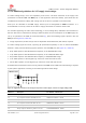


Table Of Contents
- Contents
- 1 System description
- 1.1 Overview
- 1.2 Architecture
- 1.3 Pin-out
- 1.4 Operating modes
- 1.5 Supply interfaces
- 1.5.1 Module supply input (VCC)
- 1.5.1.1 VCC supply requirements
- 1.5.1.2 VCC current consumption in 2G connected mode
- 1.5.1.3 VCC current consumption in 3G connected mode
- 1.5.1.4 VCC current consumption in LTE connected mode
- 1.5.1.5 VCC current consumption in cyclic low power idle mode / active mode
- 1.5.1.6 VCC current consumption in fixed active mode
- 1.5.2 Generic digital interfaces supply output (V_INT)
- 1.5.1 Module supply input (VCC)
- 1.6 System function interfaces
- 1.7 Antenna interfaces
- 1.8 SIM interfaces
- 1.9 Data communication interfaces
- 1.10 eMMC interface
- 1.11 Digital Audio interfaces
- 1.12 ADC interfaces
- 1.13 General Purpose Input/Output
- 1.14 Reserved pins (RSVD)
- 1.15 System features
- 1.15.1 Network indication
- 1.15.2 Jamming detection
- 1.15.3 IP modes of operation
- 1.15.4 Dual stack IPv4 and IPv6
- 1.15.5 Embedded TCP/IP and UDP/IP
- 1.15.6 Embedded FTP and FTPS
- 1.15.7 Embedded HTTP and HTTPS
- 1.15.8 SSL and TLS
- 1.15.9 Firmware update Over AT (FOAT)
- 1.15.10 Firmware update Over The Air (FOTA)
- 1.15.11 Power Saving
- 2 Design-in
- 2.1 Overview
- 2.2 Supply interfaces
- 2.2.1 Module supply (VCC)
- 2.2.1.1 General guidelines for VCC supply circuit selection and design
- 2.2.1.2 Guidelines for VCC supply circuit design using a switching regulator
- 2.2.1.3 Guidelines for VCC supply circuit design using a LDO linear regulator
- 2.2.1.4 Guidelines for VCC supply circuit design using a rechargeable battery
- 2.2.1.5 Guidelines for VCC supply circuit design using a primary battery
- 2.2.1.6 Additional guidelines for VCC supply circuit design
- 2.2.1.7 Guidelines for the external battery charging circuit
- 2.2.1.8 Guidelines for external charging and power path management circuit
- 2.2.1.9 Guidelines for removing VCC supply
- 2.2.1.10 Guidelines for VCC supply layout design
- 2.2.1.11 Guidelines for grounding layout design
- 2.2.2 Generic digital interfaces supply output (V_INT)
- 2.2.1 Module supply (VCC)
- 2.3 System functions interfaces
- 2.4 Antenna interface
- 2.5 SIM interfaces
- 2.6 Data communication interfaces
- 2.7 eMMC interface
- 2.8 Digital Audio interface
- 2.9 ADC interfaces
- 2.10 General Purpose Input/Output
- 2.11 Reserved pins (RSVD)
- 2.12 Module placement
- 2.13 Module footprint and paste mask
- 2.14 Thermal guidelines
- 2.15 Design-in checklist
- 3 Handling and soldering
- 4 Approvals
- 5 Product testing
- 6 FCC Notes
- Appendix
- Glossary
- Related documents
- Revision history
- Contact

TOBY-L3 series - System Integration Manual
TSD-19090601 - R13 System Integration Manual Page 65 of 143
Figure 22 and Table 18 show an example of a high reliability power supply circuit, where the module VCC
input is supplied by a step-down switching regulator capable of delivering maximum current with low
output ripple and with fixed switching frequency in PWM mode operation greater than 1 MHz.
12V
C5
R3
C4
R2
C2
C1
R1
VIN
RUN
VC
RT
PG
SYNC
BD
BOOST
SW
FB
GND
6
7
10
9
5
C6
1
2
3
8
11
4
C7
C8
D1
R4
R5
L1
C3
U1
TOBY-L3 series
71
VCC
72
VCC
70
VCC
GND
Figure 22: Example of high reliability VCC supply application circuit using a step-down regulator
Reference
Description
Part Number - Manufacturer
C1
10 µF Capacitor Ceramic X7R 5750 15% 50 V
C5750X7R1H106MB - TDK
C2
10 nF Capacitor Ceramic X7R 0402 10% 16 V
GRM155R71C103KA01 - Murata
C3
680 pF Capacitor Ceramic X7R 0402 10% 16 V
GRM155R71H681KA01 - Murata
C4
22 pF Capacitor Ceramic C0G 0402 5% 25 V
GRM1555C1H220JZ01 - Murata
C5
10 nF Capacitor Ceramic X7R 0402 10% 16 V
GRM155R71C103KA01 - Murata
C6
470 nF Capacitor Ceramic X7R 0603 10% 25 V
GRM188R71E474KA12 - Murata
C7
22 µF Capacitor Ceramic X5R 1210 10% 25 V
GRM32ER61E226KE15 - Murata
C8
330 µF Capacitor Tantalum D_SIZE 6.3 V 45 m
T520D337M006ATE045 - KEMET
D1
Schottky Diode 40 V 3 A
MBRA340T3G - ON Semiconductor
L1
10 µH Inductor 744066100 30% 3.6 A
744066100 - Wurth Electronics
R1
470 k Resistor 0402 5% 0.1 W
2322-705-87474-L - Yageo
R2
15 k Resistor 0402 5% 0.1 W
2322-705-87153-L - Yageo
R3
22 k Resistor 0402 5% 0.1 W
2322-705-87223-L - Yageo
R4
390 k Resistor 0402 1% 0.063 W
RC0402FR-07390KL - Yageo
R5
100 k Resistor 0402 5% 0.1 W
2322-705-70104-L - Yageo
U1
Step-Down Regulator MSOP10 3.5 A 2.4 MHz
LT3972IMSE#PBF - Linear Technology
Table 18: Components for high reliability VCC supply application circuit using a step-down regulator
☞ See section 2.2.1.6, in particular Figure 24 / Table 20, for the additional parts recommended for noise-
sensitive applications and/or for applications with antenna(s) placed close to the module.