
Integration Manual


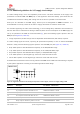


Table Of Contents
- Contents
- 1 System description
- 1.1 Overview
- 1.2 Architecture
- 1.3 Pin-out
- 1.4 Operating modes
- 1.5 Supply interfaces
- 1.5.1 Module supply input (VCC)
- 1.5.1.1 VCC supply requirements
- 1.5.1.2 VCC current consumption in 2G connected mode
- 1.5.1.3 VCC current consumption in 3G connected mode
- 1.5.1.4 VCC current consumption in LTE connected mode
- 1.5.1.5 VCC current consumption in cyclic low power idle mode / active mode
- 1.5.1.6 VCC current consumption in fixed active mode
- 1.5.2 Generic digital interfaces supply output (V_INT)
- 1.5.1 Module supply input (VCC)
- 1.6 System function interfaces
- 1.7 Antenna interfaces
- 1.8 SIM interfaces
- 1.9 Data communication interfaces
- 1.10 eMMC interface
- 1.11 Digital Audio interfaces
- 1.12 ADC interfaces
- 1.13 General Purpose Input/Output
- 1.14 Reserved pins (RSVD)
- 1.15 System features
- 1.15.1 Network indication
- 1.15.2 Jamming detection
- 1.15.3 IP modes of operation
- 1.15.4 Dual stack IPv4 and IPv6
- 1.15.5 Embedded TCP/IP and UDP/IP
- 1.15.6 Embedded FTP and FTPS
- 1.15.7 Embedded HTTP and HTTPS
- 1.15.8 SSL and TLS
- 1.15.9 Firmware update Over AT (FOAT)
- 1.15.10 Firmware update Over The Air (FOTA)
- 1.15.11 Power Saving
- 2 Design-in
- 2.1 Overview
- 2.2 Supply interfaces
- 2.2.1 Module supply (VCC)
- 2.2.1.1 General guidelines for VCC supply circuit selection and design
- 2.2.1.2 Guidelines for VCC supply circuit design using a switching regulator
- 2.2.1.3 Guidelines for VCC supply circuit design using a LDO linear regulator
- 2.2.1.4 Guidelines for VCC supply circuit design using a rechargeable battery
- 2.2.1.5 Guidelines for VCC supply circuit design using a primary battery
- 2.2.1.6 Additional guidelines for VCC supply circuit design
- 2.2.1.7 Guidelines for the external battery charging circuit
- 2.2.1.8 Guidelines for external charging and power path management circuit
- 2.2.1.9 Guidelines for removing VCC supply
- 2.2.1.10 Guidelines for VCC supply layout design
- 2.2.1.11 Guidelines for grounding layout design
- 2.2.2 Generic digital interfaces supply output (V_INT)
- 2.2.1 Module supply (VCC)
- 2.3 System functions interfaces
- 2.4 Antenna interface
- 2.5 SIM interfaces
- 2.6 Data communication interfaces
- 2.7 eMMC interface
- 2.8 Digital Audio interface
- 2.9 ADC interfaces
- 2.10 General Purpose Input/Output
- 2.11 Reserved pins (RSVD)
- 2.12 Module placement
- 2.13 Module footprint and paste mask
- 2.14 Thermal guidelines
- 2.15 Design-in checklist
- 3 Handling and soldering
- 4 Approvals
- 5 Product testing
- 6 FCC Notes
- Appendix
- Glossary
- Related documents
- Revision history
- Contact

TOBY-L3 series - System Integration Manual
TSD-19090601 - R13 System Integration Manual Page 63 of 143
Main Supply
Available?
Battery
Li-Ion 3.7 V
Linear LDO
Regulator
Main Supply
Voltage > 4.2V?
Switching Step-
Down Regulator
No, portable device
No, less than 4.2 V
Yes, greater than 4.2 V
Yes, always available
Figure 21: VCC supply concept selection
The switching step-down regulator is the typical choice when the available primary supply source has a
nominal voltage much higher (e.g. greater than 4.2 V) than the operating supply voltage of TOBY-L3 series.
The use of switching step-down provides the best power efficiency for the overall application and minimizes
current drawn from the main supply source. See sections 2.2.1.2, 2.2.1.6, 2.2.1.10, 2.2.1.11 for specific design-
in.
The use of an LDO linear regulator becomes convenient for a primary supply with a relatively low voltage
(e.g. less or equal than 4.2). In this case the typical 90% efficiency of the switching regulator diminishes the
benefit of voltage step-down and no true advantage is gained in input current savings. On the opposite
side, linear regulators are not recommended for high voltage step-down as they dissipate a considerable
amount of energy in thermal power. See sections 2.2.1.3, 2.2.1.6, 2.2.1.10, 2.2.1.11 for specific design-in.
If TOBY-L3 series modules are deployed in a mobile unit where no permanent primary supply source is
available, then a battery will be required to provide VCC. A standard 3-cell Li-Ion or Li-Pol battery pack
directly connected to VCC is the usual choice for battery-powered devices. During charging, batteries with
Ni-MH chemistry typically reach a maximum voltage that is above the maximum rating for VCC, and should
therefore be avoided. See sections 2.2.1.4, 2.2.1.6, 2.2.1.10, 2.2.1.11 for specific design-in.
Keep in mind that the use of rechargeable batteries requires the implementation of a suitable charger circuit
which is not included in the modules. The charger circuit must be designed to prevent over-voltage on VCC
pins, and it should be selected according to the application requirements: a DC/DC switching charger is the
typical choice when the charging source has an high nominal voltage (e.g. ~12 V), whereas a linear charger
is the typical choice when the charging source has a relatively low nominal voltage (~5 V). If both a
permanent primary supply / charging source (e.g. ~12 V) and a rechargeable back-up battery (e.g. 3.7 V Li-
Pol) are available at the same time as possible supply source, then a suitable charger / regulator with
integrated power path management function can be selected to supply the module while simultaneously
and independently charging the battery. See sections 2.2.1.7, 2.2.1.8, and 2.2.1.4, 2.2.1.6, 2.2.1.10, 2.2.1.11
for specific design-in.
An appropriate primary (not rechargeable) battery can be selected taking into account the maximum current
specified in the TOBY-L3 series Data Sheet [1] during connected mode, considering that primary cells might
have weak power capability. See sections 2.2.1.5, and 2.2.1.6, 2.2.1.10, 2.2.1.11 for specific design-in.