
Integration Manual


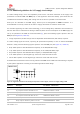


Table Of Contents
- Contents
- 1 System description
- 1.1 Overview
- 1.2 Architecture
- 1.3 Pin-out
- 1.4 Operating modes
- 1.5 Supply interfaces
- 1.5.1 Module supply input (VCC)
- 1.5.1.1 VCC supply requirements
- 1.5.1.2 VCC current consumption in 2G connected mode
- 1.5.1.3 VCC current consumption in 3G connected mode
- 1.5.1.4 VCC current consumption in LTE connected mode
- 1.5.1.5 VCC current consumption in cyclic low power idle mode / active mode
- 1.5.1.6 VCC current consumption in fixed active mode
- 1.5.2 Generic digital interfaces supply output (V_INT)
- 1.5.1 Module supply input (VCC)
- 1.6 System function interfaces
- 1.7 Antenna interfaces
- 1.8 SIM interfaces
- 1.9 Data communication interfaces
- 1.10 eMMC interface
- 1.11 Digital Audio interfaces
- 1.12 ADC interfaces
- 1.13 General Purpose Input/Output
- 1.14 Reserved pins (RSVD)
- 1.15 System features
- 1.15.1 Network indication
- 1.15.2 Jamming detection
- 1.15.3 IP modes of operation
- 1.15.4 Dual stack IPv4 and IPv6
- 1.15.5 Embedded TCP/IP and UDP/IP
- 1.15.6 Embedded FTP and FTPS
- 1.15.7 Embedded HTTP and HTTPS
- 1.15.8 SSL and TLS
- 1.15.9 Firmware update Over AT (FOAT)
- 1.15.10 Firmware update Over The Air (FOTA)
- 1.15.11 Power Saving
- 2 Design-in
- 2.1 Overview
- 2.2 Supply interfaces
- 2.2.1 Module supply (VCC)
- 2.2.1.1 General guidelines for VCC supply circuit selection and design
- 2.2.1.2 Guidelines for VCC supply circuit design using a switching regulator
- 2.2.1.3 Guidelines for VCC supply circuit design using a LDO linear regulator
- 2.2.1.4 Guidelines for VCC supply circuit design using a rechargeable battery
- 2.2.1.5 Guidelines for VCC supply circuit design using a primary battery
- 2.2.1.6 Additional guidelines for VCC supply circuit design
- 2.2.1.7 Guidelines for the external battery charging circuit
- 2.2.1.8 Guidelines for external charging and power path management circuit
- 2.2.1.9 Guidelines for removing VCC supply
- 2.2.1.10 Guidelines for VCC supply layout design
- 2.2.1.11 Guidelines for grounding layout design
- 2.2.2 Generic digital interfaces supply output (V_INT)
- 2.2.1 Module supply (VCC)
- 2.3 System functions interfaces
- 2.4 Antenna interface
- 2.5 SIM interfaces
- 2.6 Data communication interfaces
- 2.7 eMMC interface
- 2.8 Digital Audio interface
- 2.9 ADC interfaces
- 2.10 General Purpose Input/Output
- 2.11 Reserved pins (RSVD)
- 2.12 Module placement
- 2.13 Module footprint and paste mask
- 2.14 Thermal guidelines
- 2.15 Design-in checklist
- 3 Handling and soldering
- 4 Approvals
- 5 Product testing
- 6 FCC Notes
- Appendix
- Glossary
- Related documents
- Revision history
- Contact

TOBY-L3 series - System Integration Manual
TSD-19090601 - R13 System Integration Manual Page 61 of 143
2 Design-in
2.1 Overview
For optimal integration of the modules in the application PCB, follow the design guidelines stated in this
section.
Every application circuit must be properly designed to guarantee the correct functionality of the relative
interface, but a number of points require greater attention during the design of the application device.
The following list provides a rank of importance in the application design, starting with the most significant:
1. Module antenna connection:
Antenna circuit directly affects the RF compliance of the device integrating a TOBY-L3 series module
with applicable certification schemes. Very carefully follow the suggestions provided in section 2.4 for
the schematic and layout design.
2. Module supply:
The supply circuit affects the RF compliance of the device integrating a TOBY-L3 series module with
applicable required certification schemes as well as the antenna circuit design. Very carefully follow
the suggestions provided in section 2.2.1 for the schematic and layout design.
3. USB interface:
Accurate design is required to guarantee USB functionality. Carefully follow the suggestions provided
in section 2.6.1 for the schematic and layout design.
4. SIM interface:
Accurate design is required to guarantee SIM card functionality reducing the risk of RF coupling.
Carefully follow the suggestions provided in section 2.5 for the schematic and layout design.
5. System functions:
Accurate design is required to guarantee well defined voltage level during operation at Reset and
Power-on inputs. Carefully follow the suggestions provided in section 2.3 for the schematic and layout
design.
6. Digital Audio:
Accurate design is required to obtain clear and high quality audio reducing the risk of noise from
audio lines due to both supply burst noise coupling and RF detection. Carefully follow the suggestions
provided in section 2.8 for the schematic and layout design.
7. SDIO, SGMII, eMMC interfaces:
Accurate design is required to guarantee SDIO, SGMII, eMMC interfaces functionality. Carefully follow
the suggestions provided in section 2.6.5, 2.6.6, 2.7 for the schematic and layout design.
8. ADC interfaces:
Accurate design is required to guarantee ADC interfaces functionality. Carefully follow the suggestions
provided in section 2.9 for the schematic and layout design.