
Integration Manual

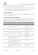

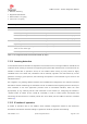


Table Of Contents
- Contents
- 1 System description
- 1.1 Overview
- 1.2 Architecture
- 1.3 Pin-out
- 1.4 Operating modes
- 1.5 Supply interfaces
- 1.5.1 Module supply input (VCC)
- 1.5.1.1 VCC supply requirements
- 1.5.1.2 VCC current consumption in 2G connected mode
- 1.5.1.3 VCC current consumption in 3G connected mode
- 1.5.1.4 VCC current consumption in LTE connected mode
- 1.5.1.5 VCC current consumption in cyclic low power idle mode / active mode
- 1.5.1.6 VCC current consumption in fixed active mode
- 1.5.2 Generic digital interfaces supply output (V_INT)
- 1.5.1 Module supply input (VCC)
- 1.6 System function interfaces
- 1.7 Antenna interfaces
- 1.8 SIM interfaces
- 1.9 Data communication interfaces
- 1.10 eMMC interface
- 1.11 Digital Audio interfaces
- 1.12 ADC interfaces
- 1.13 General Purpose Input/Output
- 1.14 Reserved pins (RSVD)
- 1.15 System features
- 1.15.1 Network indication
- 1.15.2 Jamming detection
- 1.15.3 IP modes of operation
- 1.15.4 Dual stack IPv4 and IPv6
- 1.15.5 Embedded TCP/IP and UDP/IP
- 1.15.6 Embedded FTP and FTPS
- 1.15.7 Embedded HTTP and HTTPS
- 1.15.8 SSL and TLS
- 1.15.9 Firmware update Over AT (FOAT)
- 1.15.10 Firmware update Over The Air (FOTA)
- 1.15.11 Power Saving
- 2 Design-in
- 2.1 Overview
- 2.2 Supply interfaces
- 2.2.1 Module supply (VCC)
- 2.2.1.1 General guidelines for VCC supply circuit selection and design
- 2.2.1.2 Guidelines for VCC supply circuit design using a switching regulator
- 2.2.1.3 Guidelines for VCC supply circuit design using a LDO linear regulator
- 2.2.1.4 Guidelines for VCC supply circuit design using a rechargeable battery
- 2.2.1.5 Guidelines for VCC supply circuit design using a primary battery
- 2.2.1.6 Additional guidelines for VCC supply circuit design
- 2.2.1.7 Guidelines for the external battery charging circuit
- 2.2.1.8 Guidelines for external charging and power path management circuit
- 2.2.1.9 Guidelines for removing VCC supply
- 2.2.1.10 Guidelines for VCC supply layout design
- 2.2.1.11 Guidelines for grounding layout design
- 2.2.2 Generic digital interfaces supply output (V_INT)
- 2.2.1 Module supply (VCC)
- 2.3 System functions interfaces
- 2.4 Antenna interface
- 2.5 SIM interfaces
- 2.6 Data communication interfaces
- 2.7 eMMC interface
- 2.8 Digital Audio interface
- 2.9 ADC interfaces
- 2.10 General Purpose Input/Output
- 2.11 Reserved pins (RSVD)
- 2.12 Module placement
- 2.13 Module footprint and paste mask
- 2.14 Thermal guidelines
- 2.15 Design-in checklist
- 3 Handling and soldering
- 4 Approvals
- 5 Product testing
- 6 FCC Notes
- Appendix
- Glossary
- Related documents
- Revision history
- Contact

TOBY-L3 series - System Integration Manual
TSD-19090601 - R13 System Integration Manual Page 54 of 143
The modules support I
2
S transmit and I
2
S receive data 16-bit words long, linear. Data is transmitted and
read in 2’s complement notation. The MSB is transmitted and read first.
I
2
S clock signal frequency depends on the frame length, the sample rate and the selected mode of operation:
17 x <I2S_sample_rate> or 18 x <I2S_sample_rate> in PCM mode (short synchronization signal)
16 x 2 x <I2S_sample_rate> in Normal I2S mode (long synchronization signal)
1.12 ADC interfaces
TOBY-L3 series modules include Analog to Digital Converter inputs (ADC1, ADC2), which can be handled
by means of the dedicated open CPU API.
1.13 General Purpose Input/Output
TOBY-L3 series modules include 11 pins (GPIO1, GPIO2, GPIO3, GPIO4, GPIO5, GPIO6, GPIO7, GPIO8,
HOST_SELECT0, HOST_SELECT1, RI) that can be configured through AT command or the open CPU
application as general purpose input/output or to provide custom functions as summarized in Table 16.
Function
Description
Default
Configurable GPIOs
Ring Indicator
UART0 Ring Indicator functionality
RI
RI
Wi-Fi enable
Switch-on/off the external u-blox Wi-Fi module
connected to the cellular module over the SDIO
interface
GPIO6
GPIO1, GPIO2, GPIO3, GPIO4, GPIO5,
GPIO6, GPIO7, GPIO8, HOST_SELECT0,
HOST_SELECT1, RI
GNSS supply
enable
Enable/disable the supply of u-blox GNSS device
connected to the cellular module over the I2C0 interface
GPIO2
GPIO1, GPIO2, GPIO3, GPIO4, GPIO5,
GPIO6, GPIO7, GPIO8, HOST_SELECT0,
HOST_SELECT1, RI
GNSS data ready
Sense when u-blox GNSS device connected to the
module is ready for sending data over the I2C0 interface
GPIO3
GPIO3, GPIO5, HOST_SELECT0,
HOST_SELECT1, RI
External Interrupt
External Interrupt detection (module input)
-
GPIO3, GPIO5, HOST_SELECT0,
HOST_SELECT1, RI
Wake-up
Pull up the PIN to high level internally.
When the input level of the PIN is low, make the module
enter active mode from sleep mode.
-
GPIO3, GPIO5, HOST_SELECT0,
HOST_SELECT1, RI
Sleep Control
When the input level of the PIN is high, make the
module enter active mode(Wake up from sleep mode);
When the input level of the PIN is low or the PIN is in
floating, the module can enter sleep mode.
-
GPIO3, GPIO5, HOST_SELECT0,
HOST_SELECT1, RI
Sleep Status
Indicator the sleep status of the module; When the
module is in active mode, the output of the PIN is high
level; When the module is in sleep mode, the output of
the PIN is low level;
-
GPIO1, GPIO2, GPIO3, GPIO4, GPIO5,
GPIO6, GPIO7, GPIO8, HOST_SELECT0,
HOST_SELECT1, RI