
Integration Manual

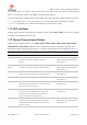


Table Of Contents
- Contents
- 1 System description
- 1.1 Overview
- 1.2 Architecture
- 1.3 Pin-out
- 1.4 Operating modes
- 1.5 Supply interfaces
- 1.5.1 Module supply input (VCC)
- 1.5.1.1 VCC supply requirements
- 1.5.1.2 VCC current consumption in 2G connected mode
- 1.5.1.3 VCC current consumption in 3G connected mode
- 1.5.1.4 VCC current consumption in LTE connected mode
- 1.5.1.5 VCC current consumption in cyclic low power idle mode / active mode
- 1.5.1.6 VCC current consumption in fixed active mode
- 1.5.2 Generic digital interfaces supply output (V_INT)
- 1.5.1 Module supply input (VCC)
- 1.6 System function interfaces
- 1.7 Antenna interfaces
- 1.8 SIM interfaces
- 1.9 Data communication interfaces
- 1.10 eMMC interface
- 1.11 Digital Audio interfaces
- 1.12 ADC interfaces
- 1.13 General Purpose Input/Output
- 1.14 Reserved pins (RSVD)
- 1.15 System features
- 1.15.1 Network indication
- 1.15.2 Jamming detection
- 1.15.3 IP modes of operation
- 1.15.4 Dual stack IPv4 and IPv6
- 1.15.5 Embedded TCP/IP and UDP/IP
- 1.15.6 Embedded FTP and FTPS
- 1.15.7 Embedded HTTP and HTTPS
- 1.15.8 SSL and TLS
- 1.15.9 Firmware update Over AT (FOAT)
- 1.15.10 Firmware update Over The Air (FOTA)
- 1.15.11 Power Saving
- 2 Design-in
- 2.1 Overview
- 2.2 Supply interfaces
- 2.2.1 Module supply (VCC)
- 2.2.1.1 General guidelines for VCC supply circuit selection and design
- 2.2.1.2 Guidelines for VCC supply circuit design using a switching regulator
- 2.2.1.3 Guidelines for VCC supply circuit design using a LDO linear regulator
- 2.2.1.4 Guidelines for VCC supply circuit design using a rechargeable battery
- 2.2.1.5 Guidelines for VCC supply circuit design using a primary battery
- 2.2.1.6 Additional guidelines for VCC supply circuit design
- 2.2.1.7 Guidelines for the external battery charging circuit
- 2.2.1.8 Guidelines for external charging and power path management circuit
- 2.2.1.9 Guidelines for removing VCC supply
- 2.2.1.10 Guidelines for VCC supply layout design
- 2.2.1.11 Guidelines for grounding layout design
- 2.2.2 Generic digital interfaces supply output (V_INT)
- 2.2.1 Module supply (VCC)
- 2.3 System functions interfaces
- 2.4 Antenna interface
- 2.5 SIM interfaces
- 2.6 Data communication interfaces
- 2.7 eMMC interface
- 2.8 Digital Audio interface
- 2.9 ADC interfaces
- 2.10 General Purpose Input/Output
- 2.11 Reserved pins (RSVD)
- 2.12 Module placement
- 2.13 Module footprint and paste mask
- 2.14 Thermal guidelines
- 2.15 Design-in checklist
- 3 Handling and soldering
- 4 Approvals
- 5 Product testing
- 6 FCC Notes
- Appendix
- Glossary
- Related documents
- Revision history
- Contact

TOBY-L3 series - System Integration Manual
TSD-19090601 - R13 System Integration Manual Page 53 of 143
1.11 Digital Audio interfaces
TOBY-L3 series modules provide a 4-wire I
2
S digital audio interface:
I2S digital audio interface, consisting of the following pins:
o I2S_TXD data output
o I2S_RXD data input
o I2S_CLK bit clock input/output
o I2S_WA world alignment / synchronization signal input/output
The I2S0 digital audio interfaces is suitable to transfer digital audio data with an external compatible digital
audio device, as an audio codec or as an audio digital signal processor.
The I
2
S interfaces can be alternatively set in different modes:
PCM mode (short synchronization signal): I
2
S word alignment signal is set high for 1 or 2 clock cycles
for the synchronization, and then is set low for 16 clock cycles according to the 17 or 18 clock cycles
frame length.
Normal I
2
S mode (long synchronization signal): I
2
S word alignment is set high / low with a 50% duty
cycle (high for 16 clock cycles / low for 16 clock cycles, according to the 32 clock cycles frame length).
The Digital Audio interface can be configured as I2S (I2S0) or PCM (PCM0) interface by means of open
CPU API or AT command, for communication with external devices with the following configuration is listed
in the Table 15:
I2S Mode (I2S0)
PCM Mode (PCM0)
I2S_TXD; I2S0 Transmit Data Out
PCM0_DOUT; PCM0 Data Out
I2S_RXD; I2S0 Receive Data In
PCM0_DIN; PCM0 Data In
I2S_CLK; I2S0 Serial Clock
PCM0_CLK; PCM0 Clock
I2S_WA; I2S0 Word Alignment
PCM0_SYNC; PCM0 Frame Sync
Table 15: TOBY-L3 series modules Digital Audio PINs configuration
The I
2
S interface can be alternatively set in 2 different roles:
Master mode
Slave mode
The sample rate of transmitted/received words, which corresponds to the I
2
S word alignment /
synchronization signal frequency (<I2S_sample_rate>), can be alternatively set to:
8 kHz
16 kHz
48 kHz