
Integration Manual

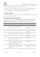


Table Of Contents
- Contents
- 1 System description
- 1.1 Overview
- 1.2 Architecture
- 1.3 Pin-out
- 1.4 Operating modes
- 1.5 Supply interfaces
- 1.5.1 Module supply input (VCC)
- 1.5.1.1 VCC supply requirements
- 1.5.1.2 VCC current consumption in 2G connected mode
- 1.5.1.3 VCC current consumption in 3G connected mode
- 1.5.1.4 VCC current consumption in LTE connected mode
- 1.5.1.5 VCC current consumption in cyclic low power idle mode / active mode
- 1.5.1.6 VCC current consumption in fixed active mode
- 1.5.2 Generic digital interfaces supply output (V_INT)
- 1.5.1 Module supply input (VCC)
- 1.6 System function interfaces
- 1.7 Antenna interfaces
- 1.8 SIM interfaces
- 1.9 Data communication interfaces
- 1.10 eMMC interface
- 1.11 Digital Audio interfaces
- 1.12 ADC interfaces
- 1.13 General Purpose Input/Output
- 1.14 Reserved pins (RSVD)
- 1.15 System features
- 1.15.1 Network indication
- 1.15.2 Jamming detection
- 1.15.3 IP modes of operation
- 1.15.4 Dual stack IPv4 and IPv6
- 1.15.5 Embedded TCP/IP and UDP/IP
- 1.15.6 Embedded FTP and FTPS
- 1.15.7 Embedded HTTP and HTTPS
- 1.15.8 SSL and TLS
- 1.15.9 Firmware update Over AT (FOAT)
- 1.15.10 Firmware update Over The Air (FOTA)
- 1.15.11 Power Saving
- 2 Design-in
- 2.1 Overview
- 2.2 Supply interfaces
- 2.2.1 Module supply (VCC)
- 2.2.1.1 General guidelines for VCC supply circuit selection and design
- 2.2.1.2 Guidelines for VCC supply circuit design using a switching regulator
- 2.2.1.3 Guidelines for VCC supply circuit design using a LDO linear regulator
- 2.2.1.4 Guidelines for VCC supply circuit design using a rechargeable battery
- 2.2.1.5 Guidelines for VCC supply circuit design using a primary battery
- 2.2.1.6 Additional guidelines for VCC supply circuit design
- 2.2.1.7 Guidelines for the external battery charging circuit
- 2.2.1.8 Guidelines for external charging and power path management circuit
- 2.2.1.9 Guidelines for removing VCC supply
- 2.2.1.10 Guidelines for VCC supply layout design
- 2.2.1.11 Guidelines for grounding layout design
- 2.2.2 Generic digital interfaces supply output (V_INT)
- 2.2.1 Module supply (VCC)
- 2.3 System functions interfaces
- 2.4 Antenna interface
- 2.5 SIM interfaces
- 2.6 Data communication interfaces
- 2.7 eMMC interface
- 2.8 Digital Audio interface
- 2.9 ADC interfaces
- 2.10 General Purpose Input/Output
- 2.11 Reserved pins (RSVD)
- 2.12 Module placement
- 2.13 Module footprint and paste mask
- 2.14 Thermal guidelines
- 2.15 Design-in checklist
- 3 Handling and soldering
- 4 Approvals
- 5 Product testing
- 6 FCC Notes
- Appendix
- Glossary
- Related documents
- Revision history
- Contact

TOBY-L3 series - System Integration Manual
TSD-19090601 - R13 System Integration Manual Page 51 of 143
Tashang has implemented special features in the cellular modules to ease the design effort for the
integration of the TOBY-L3 cellular module with a u-blox short range radio communication module, to
provide Router functionality.
The cellular modules provide additional custom functions over GPIO pins to improve the integration with
u-blox short range radio communication modules (see section 1.13). GPIO pins can handle:
“Wi-Fi enable” function provided by GPIO6, improving the power consumption of the short range radio
communication module: when the Wi-Fi functionality is not required, the external short range radio
communication module can be switched off by the cellular module
1.9.6 SGMII interface
TOBY-L3 series modules include an Ethernet Media Access Control (MAC) block supporting up to 1Gbit/s
data rate via a Serial Gigabit Media-Independent Interface compliant with the SGMII Version 1.8 specification
[8].
The module represents an Ethernet MAC controller, which can be connected to an external Ethernet physical
transceiver (PHY) chip for communication with a remote processor over Ethernet.
The following signals are provided for communication and management of an external Ethernet PHY:
V_ETH Interface supply output
SGMII_TX_P SGMII transmit-plus
SGMII_TX_N SGMII transmit-minus
SGMII_RX_P SGMII receive-plus
SGMII_RX_N SGMII receive-minus
ETH_INTR Ethernet Interrupt Input, from PHY to MAC (module input)
When this signal is high, it indicates an interrupt event in the PHY
ETH_MDIO Management Data Input Output, bidirectional signal (module input/output)
ETH_MDC Management Data Clock, from MAC to PHY (module output)