
Integration Manual


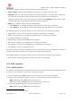


Table Of Contents
- Contents
- 1 System description
- 1.1 Overview
- 1.2 Architecture
- 1.3 Pin-out
- 1.4 Operating modes
- 1.5 Supply interfaces
- 1.5.1 Module supply input (VCC)
- 1.5.1.1 VCC supply requirements
- 1.5.1.2 VCC current consumption in 2G connected mode
- 1.5.1.3 VCC current consumption in 3G connected mode
- 1.5.1.4 VCC current consumption in LTE connected mode
- 1.5.1.5 VCC current consumption in cyclic low power idle mode / active mode
- 1.5.1.6 VCC current consumption in fixed active mode
- 1.5.2 Generic digital interfaces supply output (V_INT)
- 1.5.1 Module supply input (VCC)
- 1.6 System function interfaces
- 1.7 Antenna interfaces
- 1.8 SIM interfaces
- 1.9 Data communication interfaces
- 1.10 eMMC interface
- 1.11 Digital Audio interfaces
- 1.12 ADC interfaces
- 1.13 General Purpose Input/Output
- 1.14 Reserved pins (RSVD)
- 1.15 System features
- 1.15.1 Network indication
- 1.15.2 Jamming detection
- 1.15.3 IP modes of operation
- 1.15.4 Dual stack IPv4 and IPv6
- 1.15.5 Embedded TCP/IP and UDP/IP
- 1.15.6 Embedded FTP and FTPS
- 1.15.7 Embedded HTTP and HTTPS
- 1.15.8 SSL and TLS
- 1.15.9 Firmware update Over AT (FOAT)
- 1.15.10 Firmware update Over The Air (FOTA)
- 1.15.11 Power Saving
- 2 Design-in
- 2.1 Overview
- 2.2 Supply interfaces
- 2.2.1 Module supply (VCC)
- 2.2.1.1 General guidelines for VCC supply circuit selection and design
- 2.2.1.2 Guidelines for VCC supply circuit design using a switching regulator
- 2.2.1.3 Guidelines for VCC supply circuit design using a LDO linear regulator
- 2.2.1.4 Guidelines for VCC supply circuit design using a rechargeable battery
- 2.2.1.5 Guidelines for VCC supply circuit design using a primary battery
- 2.2.1.6 Additional guidelines for VCC supply circuit design
- 2.2.1.7 Guidelines for the external battery charging circuit
- 2.2.1.8 Guidelines for external charging and power path management circuit
- 2.2.1.9 Guidelines for removing VCC supply
- 2.2.1.10 Guidelines for VCC supply layout design
- 2.2.1.11 Guidelines for grounding layout design
- 2.2.2 Generic digital interfaces supply output (V_INT)
- 2.2.1 Module supply (VCC)
- 2.3 System functions interfaces
- 2.4 Antenna interface
- 2.5 SIM interfaces
- 2.6 Data communication interfaces
- 2.7 eMMC interface
- 2.8 Digital Audio interface
- 2.9 ADC interfaces
- 2.10 General Purpose Input/Output
- 2.11 Reserved pins (RSVD)
- 2.12 Module placement
- 2.13 Module footprint and paste mask
- 2.14 Thermal guidelines
- 2.15 Design-in checklist
- 3 Handling and soldering
- 4 Approvals
- 5 Product testing
- 6 FCC Notes
- Appendix
- Glossary
- Related documents
- Revision history
- Contact

TOBY-L3 series - System Integration Manual
TSD-19090601 - R13 System Integration Manual Page 47 of 143
asserted when one of the configured events occur and it remains asserted for 1 s unless another configured
event will happen, with the same behavior illustrated in Figure 19.
The RI function can be alternatively configured by GPIO by an AT command.
Figure 20: RI behavior at wake up host in mode 2
As described in Figure 20, the RI line can wake up the external host after configured the pin as mode 2 by
AT command.
The UART0 interface can be alternatively, in mutually exclusive way, configured as SPI (SPI1) interface by
means of open CPU API or AT command (see the TOBY-L3 series AT Commands Manual [2]), for
communication with external devices with the following configuration Table 13:
4-wire UART Mode (UART0)
SPI Mode (SPI1)
RXD (Module output); UART0 Receive Data
SPI1_MOSI; SPI1 MOSI Pin (Module Output)
TXD (Module Input); UART0 Transmit Data
SPI1_MISO; SPI1 MISO Pin (Module Input)
CTS (Module Output); UART0 Clear To Send
SPI1_SCLK; SPI1 Clock Pin (Module Output)
RTS (Module Input); UART0 Ready To Send
SPI1_CS; SPI1 Chip Select Pin (Module Output)
Table 12: TOBY-L3 series modules UART0 PINs configuration
1.9.2.2 UART1 interface
The UART1 Universal Asynchronous Receiver/Transmitter serial interface, with CMOS compatible signal levels
(0 V for ON / active state and 1.8 V for OFF / idle state), can operate as a serial interface for communication
with external devices by means of the open CPU API, with the following pins:
RXD1 module output and TXD1 module input data lines
CTS1 module output and RTS1 module input hardware flow control lines
The UART1 interface can operate at 300bit/s, 600bit/s, 1.2kbit/s, 2.4kbit/s, 4.8kbit/s, 9.6kbit/s, 19.2kbit/s,
38.4kbit/s, 57.6kbit/s, 115.2kbit/s, 230.4kbit/s, 1Mbit/s, 3Mbit/s, 4Mbit/s baud rates, with 8N1 frame format
(illustrated in Figure 17), and with hardware flow control output (CTS1 line) driven to the OFF state when
the module is not prepared to accept data by the UART1 interface.
Wake up host
time [s]
0
RI ON
RI OFF
120ms
time [s]
0
RI ON
RI OFF