
Integration Manual


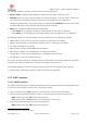


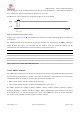


Table Of Contents
- Contents
- 1 System description
- 1.1 Overview
- 1.2 Architecture
- 1.3 Pin-out
- 1.4 Operating modes
- 1.5 Supply interfaces
- 1.5.1 Module supply input (VCC)
- 1.5.1.1 VCC supply requirements
- 1.5.1.2 VCC current consumption in 2G connected mode
- 1.5.1.3 VCC current consumption in 3G connected mode
- 1.5.1.4 VCC current consumption in LTE connected mode
- 1.5.1.5 VCC current consumption in cyclic low power idle mode / active mode
- 1.5.1.6 VCC current consumption in fixed active mode
- 1.5.2 Generic digital interfaces supply output (V_INT)
- 1.5.1 Module supply input (VCC)
- 1.6 System function interfaces
- 1.7 Antenna interfaces
- 1.8 SIM interfaces
- 1.9 Data communication interfaces
- 1.10 eMMC interface
- 1.11 Digital Audio interfaces
- 1.12 ADC interfaces
- 1.13 General Purpose Input/Output
- 1.14 Reserved pins (RSVD)
- 1.15 System features
- 1.15.1 Network indication
- 1.15.2 Jamming detection
- 1.15.3 IP modes of operation
- 1.15.4 Dual stack IPv4 and IPv6
- 1.15.5 Embedded TCP/IP and UDP/IP
- 1.15.6 Embedded FTP and FTPS
- 1.15.7 Embedded HTTP and HTTPS
- 1.15.8 SSL and TLS
- 1.15.9 Firmware update Over AT (FOAT)
- 1.15.10 Firmware update Over The Air (FOTA)
- 1.15.11 Power Saving
- 2 Design-in
- 2.1 Overview
- 2.2 Supply interfaces
- 2.2.1 Module supply (VCC)
- 2.2.1.1 General guidelines for VCC supply circuit selection and design
- 2.2.1.2 Guidelines for VCC supply circuit design using a switching regulator
- 2.2.1.3 Guidelines for VCC supply circuit design using a LDO linear regulator
- 2.2.1.4 Guidelines for VCC supply circuit design using a rechargeable battery
- 2.2.1.5 Guidelines for VCC supply circuit design using a primary battery
- 2.2.1.6 Additional guidelines for VCC supply circuit design
- 2.2.1.7 Guidelines for the external battery charging circuit
- 2.2.1.8 Guidelines for external charging and power path management circuit
- 2.2.1.9 Guidelines for removing VCC supply
- 2.2.1.10 Guidelines for VCC supply layout design
- 2.2.1.11 Guidelines for grounding layout design
- 2.2.2 Generic digital interfaces supply output (V_INT)
- 2.2.1 Module supply (VCC)
- 2.3 System functions interfaces
- 2.4 Antenna interface
- 2.5 SIM interfaces
- 2.6 Data communication interfaces
- 2.7 eMMC interface
- 2.8 Digital Audio interface
- 2.9 ADC interfaces
- 2.10 General Purpose Input/Output
- 2.11 Reserved pins (RSVD)
- 2.12 Module placement
- 2.13 Module footprint and paste mask
- 2.14 Thermal guidelines
- 2.15 Design-in checklist
- 3 Handling and soldering
- 4 Approvals
- 5 Product testing
- 6 FCC Notes
- Appendix
- Glossary
- Related documents
- Revision history
- Contact

TOBY-L3 series - System Integration Manual
TSD-19090601 - R13 System Integration Manual Page 46 of 143
The RI line can notify an incoming call: the line is switched from the OFF state to the ON state with a 4:1
duty cycle and a 5 s period (ON for 1 s, OFF for 4 s, see Figure 18), until the DTE attached to the module
sends the ATA string and the module accepts the incoming data call. The RING string sent by the module
(DCE) to the serial port at constant time intervals is not correlated with the switch of the Ring Indicator
line to the ON state.
Figure 18: RI behavior during an incoming call
The RI output line can notify an SMS arrival. When the SMS arrives, the line switches from OFF to ON for
1 s (see Figure 19), if the feature is enabled by the AT+CNMI command (see the TOBY-L3 series AT
Commands Manual [2]).
Figure 19: RI behavior at SMS arrival
This behavior allows the DTE to stay in power saving mode until the DCE related event requests service.
For SMS arrival, if several events coincidently occur or in quick succession, each event independently triggers
the RI line, although the line will not be deactivated between each event. As a result, the RI line may stay
to ON for more than 1 s, if an incoming call is answered within less than 1 s (with ATA or if auto-answering
is set to ATS0=1) then the RI line is set to OFF earlier, so that:
☞ RI line monitoring cannot be used by the DTE to determine the number of received SMSs.
☞ For multiple events (incoming call plus SMS received), the RI line cannot be used to discriminate the
two events, but the DTE must rely on subsequent URCs and interrogate the DCE with the suitable
commands.
The RI line can additionally notify all the URCs and responses, if the feature is enabled by the specific
AT+URING command (for more details, see the TOBY-L3 series AT Commands Manual [2]): the RI line is
1s
time [s]
151050
RI ON
RI OFF
Call incomes
1s
time [s]
151050
RI ON
RI OFF
Call incomes
SMS arrives
time [s]
0
RI ON
RI OFF
1s
time [s]
0
RI ON
RI OFF
1s